
Semiconductor chip and semiconductor package having the same

a semiconductor chip and chip technology, applied in the field of semiconductor devices, can solve the problems of affecting the reliability of electronic appliances manufactured using semiconductor chips, affecting the reliability of electronic appliances, etc., to improve the emi (electro-magnetic interference) characteristic, and improve the effect of emi

Active Publication Date: 2015-11-10
SK HYNIX INC
View PDF7 Cites 0 Cited by
  • Summary
  • Abstract
  • Description
  • Claims
  • Application Information

AI Technical Summary

Benefits of technology

[0008]Various embodiments are directed to a semiconductor chip suitable for improving an EMI (electro-magnetic interference) characteristic and accomplishing light weight, slimness, compactness and miniaturization.

Problems solved by technology

Recently, as the operation speed of a semiconductor device increases, a large amount of electro-magnetic waves is generated in a semiconductor chip, so the reliability of an electronic appliance manufactured using the semiconductor chip is likely to deteriorate.
In the case where such a semiconductor chip is used in an electronic appliance, as the electro-magnetic waves generated from the semiconductor chip are radiated, electro-magnetic interference (EMI) may be caused in other electronic products which are mounted to the electronic appliance.
As a consequence, electro-magnetic noise or a fail such as a mis-operation may be caused in the electronic appliance in which the semiconductor chip is used, whereby the reliability of the electronic appliance may be degraded.
In particular, as the responding speed of the semiconductor chip increases and the semiconductor chip has high capacity, the problem of the electro-magnetic interference due to the radiation of electro-magnetic waves becomes serious.
However, even in this case, a problem is caused in that the size of the semiconductor package increases due to the presence of the shielding layer formed on the molding part of the semiconductor package.
In addition, it is impossible to solve the problem of the electro-magnetic interference between semiconductor chips and between a semiconductor chip and a substrate in the semiconductor package.

Method used


Image

  • Semiconductor chip and semiconductor package having the same
  • Semiconductor chip and semiconductor package having the same
  • Semiconductor chip and semiconductor package having the same

Examples


Embodiment Construction

[0035]Hereafter, various embodiments will be described in detail with reference to the accompanying drawings.

[0036]It is to be understood herein that the drawings are not necessarily to scale and in some instances proportions may have been exaggerated in order to more clearly depict certain features of the invention.

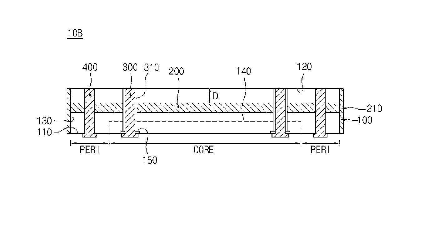
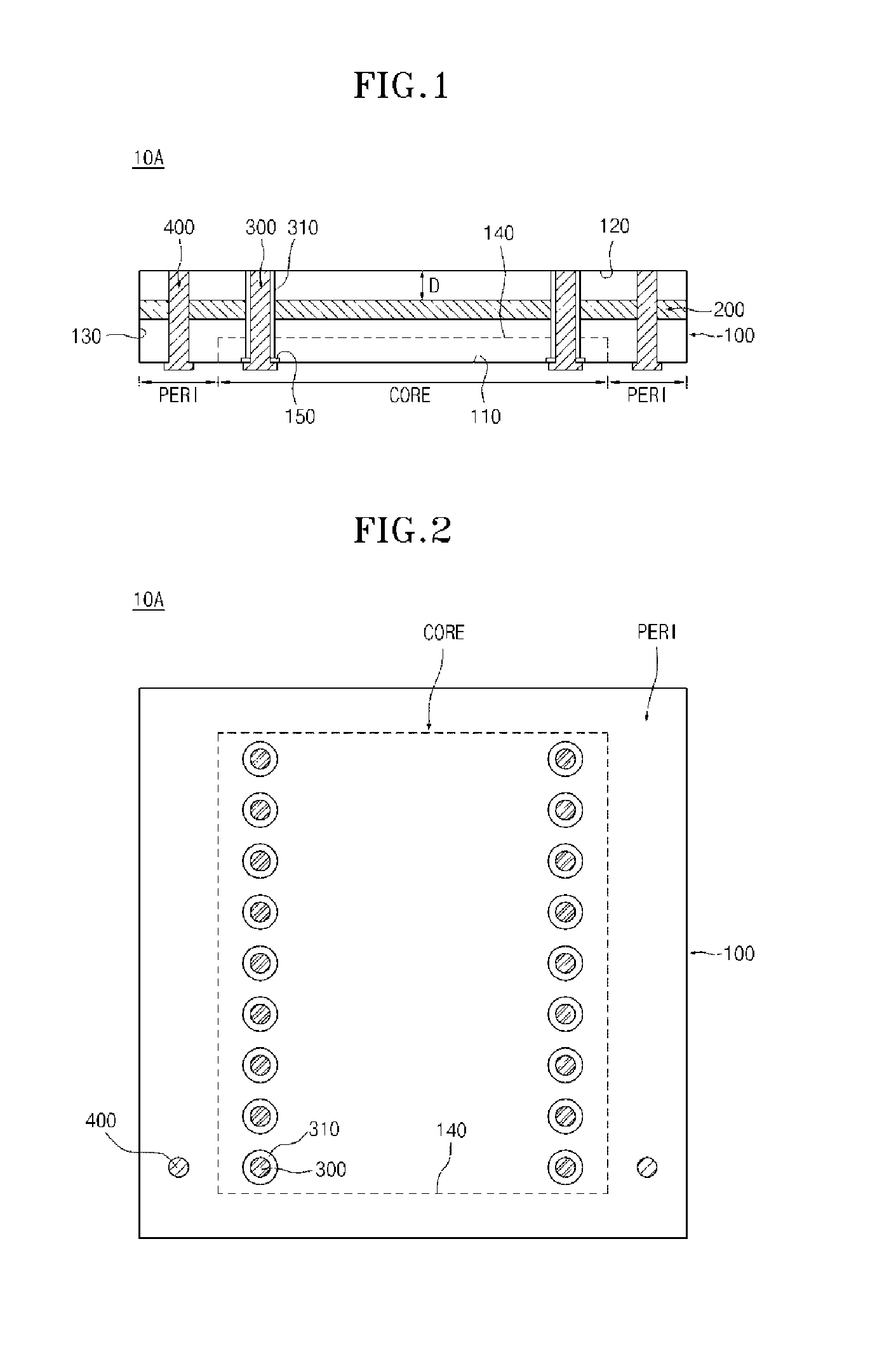
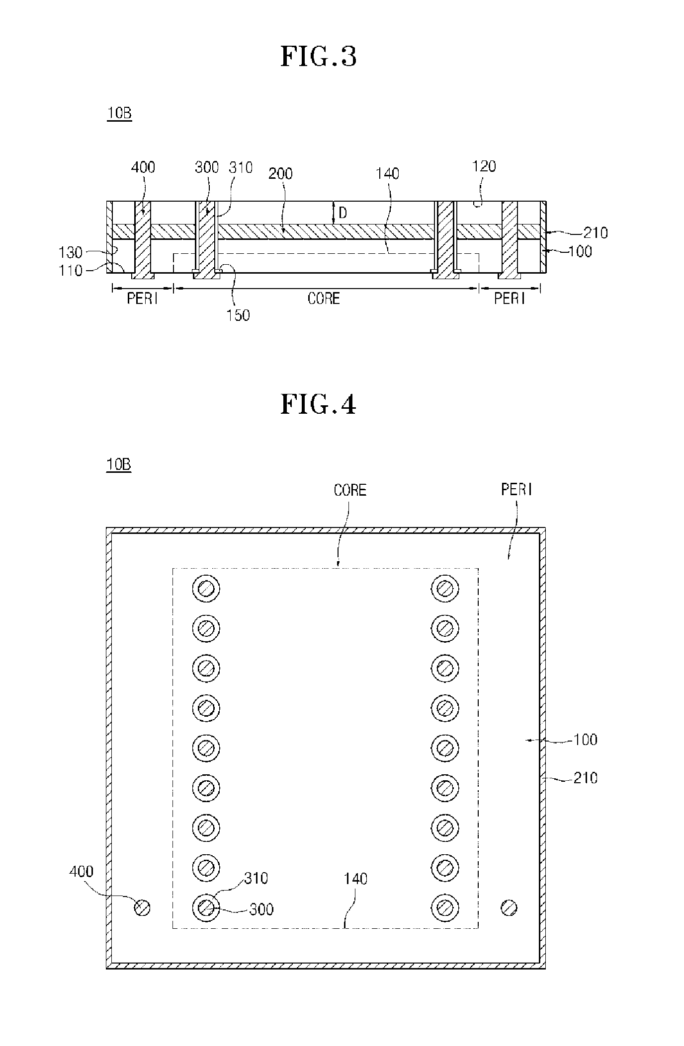
[0037]FIG. 1 is a cross-sectional view illustrating a semiconductor chip in accordance with an embodiment, and FIG. 2 is a plan view illustrating the semiconductor chip of FIG. 1.

[0038]In an embodiment associated with FIGS. 1 and 2, the semiconductor chip 10A may include a semiconductor substrate 100 and a shielding layer 200. Besides, the semiconductor chip 10A further may include first through electrodes 300 and second through electrodes 400.

[0039]The semiconductor substrate 100 may be divided into a core region CORE and a peripheral region PERI, and may have one surface 110, the other surface 120, side surfaces 130, an integrated circuit 140 and bonding pads 150.

[0040...


PUM


Abstract

A semiconductor chip includes a semiconductor substrate having one surface, the other surface which faces away from the one surface, and an integrated circuit which is formed on the one surface; and a shielding layershielding layer formed in the semiconductor substrate to correspond to the other surface.

Description

CROSS-REFERENCE TO RELATED APPLICATIONS[0001]The present application claims priority under 35 U.S.C. 119(a) to Korean Patent Application Number 10-2012-95311 filed in the Korean intellectual property office on Aug. 30, 2012, which is incorporated herein by reference in its entirety.BACKGROUND[0002]1. Field of the Invention[0003]The present invention generally relates to a semiconductor device, and more particularly, to a semiconductor chip suitable for improving an EMI (electro-magnetic interference) characteristic and a semiconductor package having the same.[0004]2. Description of the Related Art[0005]These days, the electronic industry trends to manufacture products at reduced costs with high reliability in such a way as to accomplish light weight, miniaturization, high speed operation, multi-functionality and high performance. A package assembly technology is considered as one of important technologies for achieving purposes of designing such products. The package assembly techno...

Claims


Application Information

Patent Timeline
Patent Type & Authority Patents(United States)
IPC IPC(8): H01L23/552H01L23/48H01L25/065H01L23/538
CPCH01L23/552H01L23/481H01L25/0657H01L23/5384H01L2224/0401H01L2224/05552H01L2224/05572H01L2224/13025H01L2224/16145H01L2224/16225H01L2224/32145H01L2224/32225H01L2224/73204H01L2225/06513H01L2225/06517H01L2225/06537H01L2225/06565H01L2924/00014H01L2924/15311H01L2924/00012H01L2924/00H01L23/60H05K9/00
Inventor LEE, SEUNG YEOP
Owner SK HYNIX INC
Learn More