Three-dimensional semiconductor memory device and a method of manufacturing the same

a semiconductor memory and three-dimensional technology, applied in the field of three-dimensional semiconductor memory devices, can solve the problem that the available area of the two-dimensional or planar semiconductor memory devices may be limited, and achieve the effect of improving the integration degree and reliability

Inactive Publication Date: 2014-02-20
SAMSUNG ELECTRONICS CO LTD
View PDF2 Cites 51 Cited by
  • Summary
  • Abstract
  • Description
  • Claims
  • Application Information

AI Technical Summary

Benefits of technology

[0007]Exemplary embodiments of the inventive concept may provide three-dimensional (3D) semiconductor memory devices capable of improving integration degree and reliability.

Problems solved by technology

However, even with the high integration density afforded by increased pattern fineness, the capacity of the two-dimensional or planar semiconductor memory devices may be limited by its available area.

Method used


Image

  • Three-dimensional semiconductor memory device and a method of manufacturing the same
  • Three-dimensional semiconductor memory device and a method of manufacturing the same
  • Three-dimensional semiconductor memory device and a method of manufacturing the same

Examples


Embodiment Construction

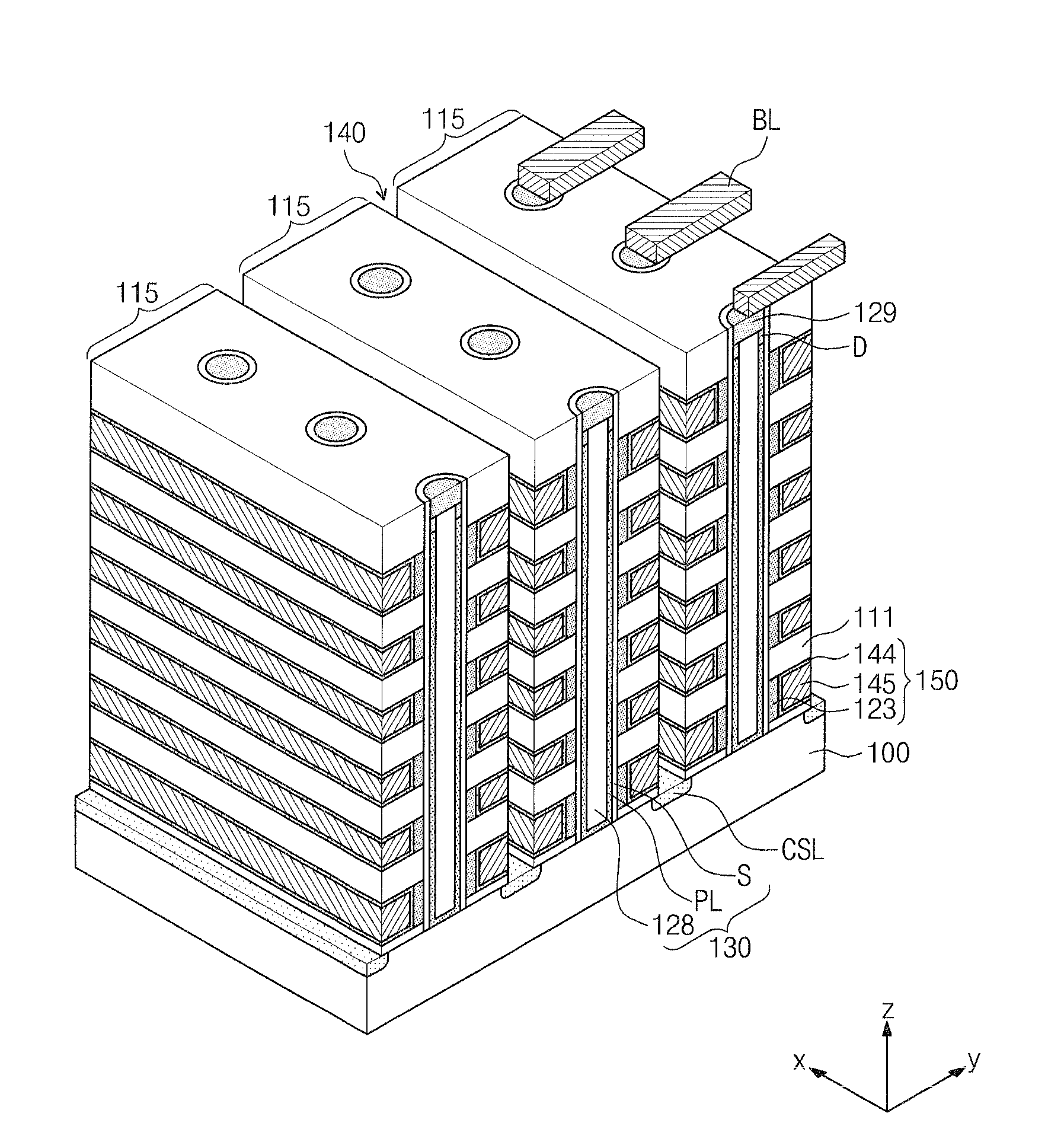
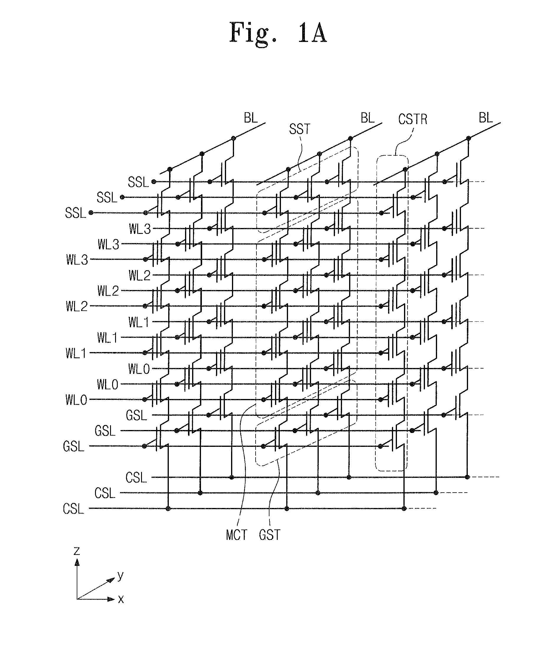
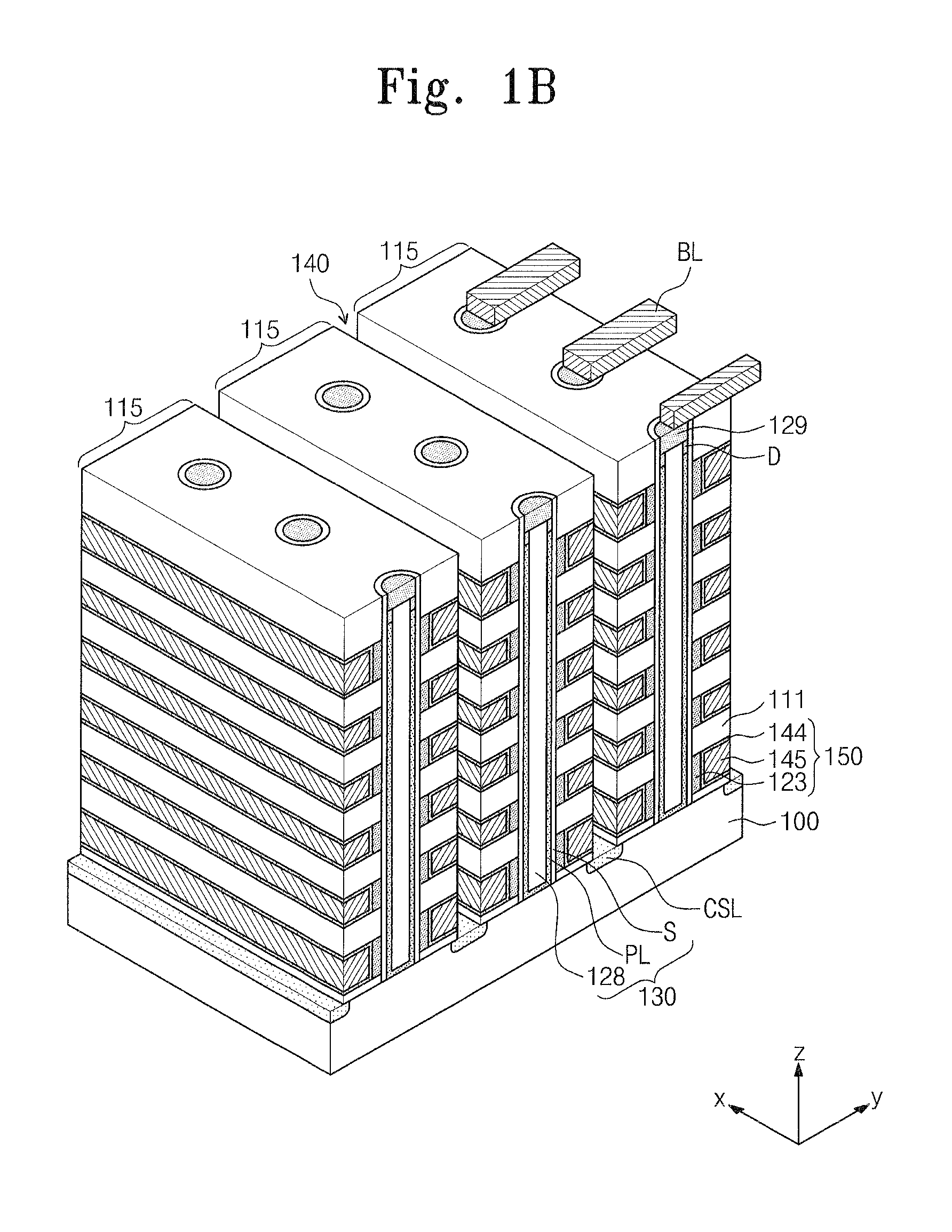
[0037]Hereinafter, exemplary embodiments of the inventive concept will be described in detail with reference to the accompanying drawings. It should be noted, however, that the inventive concept is not limited to the following exemplary embodiments, and may be embodied in various forms. In the drawings, certain aspects of embodiments of the inventive concept such as sizes of elements may be exaggerated for clarity.

[0038]As used herein, the singular forms “a,”“an” and “the” are intended to include the plural forms as well, unless the context clearly indicates otherwise. It will be understood that when an element such as a layer, region or substrate is referred to as being “connected” or “coupled” to another element, it may be directly connected or coupled to the other element or intervening elements may be present.

[0039]Similarly, it will be understood that when an element such as a layer, region or substrate is referred to as being “on” another element, it can be directly on the oth...


PUM


Abstract

A three-dimensional (3D) semiconductor memory device may include an electrode structure extending in a first direction and including insulating patterns and horizontal electrodes stacked on a substrate, a semiconductor pillar penetrating the electrode structure and connected to the substrate, a charge storage layer between the semiconductor pillar and the electrode structure, a tunnel insulating layer between the charge storage layer and the semiconductor pillar, and a blocking insulating layer between the charge storage layer and the electrode structure. A first horizontal electrode of the horizontal electrodes includes a gate electrode and a metal stopper between the gate electrode and the blocking insulating layer.

Description

CROSS-REFERENCE TO RELATED APPLICATION[0001]This U.S. non-provisional patent application claims priority under 35 U.S.C. §119 to Korean Patent Application No. 10-2012-0090849, filed on Aug. 20, 2012, in the Korean Intellectual Property Office, the disclosure of which is incorporated by reference herein in its entirety.BACKGROUND[0002]1. Technical Field[0003]The inventive concept relates to semiconductor devices and methods of manufacturing the same and, more particularly, to three-dimensional semiconductor memory devices including vertically stacked memory cells and methods of manufacturing the same.[0004]2. Discussion of the Related Art[0005]Demand for highly integrated semiconductor memory devices has been increasing. To make semiconductor memory devices such as two-dimensional or planar semiconductor memory devices further integrated, fine pattern forming technology may be used. However, even with the high integration density afforded by increased pattern fineness, the capacity o...

Claims


Application Information

Patent Timeline
Patent Type & Authority Applications(United States)
IPC IPC(8): H01L29/792
CPCH01L29/7926H01L29/66833H10B43/27H01L21/76205H01L21/823487
Inventor KIM, JUHYUNGSHIN, YOOCHEOL
Owner SAMSUNG ELECTRONICS CO LTD
Why Eureka
Try Eureka