Integrated-optical microsystem based on organic semiconductors

a technology of organic semiconductors and optical microsystems, applied in the direction of thermoelectric devices, basic electric elements, electric apparatus, etc., can solve the problems of generating light within the same material used for the rest of the photosensitive and electronic devices, and achieve the effects of avoiding assembly costs, and reducing the production cost of optical microsystems

Inactive Publication Date: 2006-05-02
CSEM CENT SUISSE DELECTRONIQUE & DE MICROTECHNIQUE SA RECH & DEV
View PDF8 Cites 31 Cited by
  • Summary
  • Abstract
  • Description
  • Claims
  • Application Information

AI Technical Summary

Benefits of technology

[0013]It is an object of the invention to provide an integrated-optical microsystem based on organic semiconductors and a method of manufacturing such integrated-optical microsystem which overcome the limitations of the prior art. In particular, it is an object to manufacture the complete optical microsystem with one single process, avoiding cost for assembly and further hybrid system integration. Another object is to scale up the manufacturing process to very large surfaces of square meters. Still another object is to significantly reduce the production costs of optical microsystems compared with the prior art. Yet another object is to shape the resulting microsystems in three dimensions after an essentially planar fabrication. Still another object is to achieve a higher degree of integration, of functionality, and of system complexity than with the prior art.

Problems solved by technology

Due to the semiconductor properties of silicon it is difficult, however, to generate light within the same material used for the rest of the photosensitive and electronic devices.

Method used


Image

  • Integrated-optical microsystem based on organic semiconductors
  • Integrated-optical microsystem based on organic semiconductors
  • Integrated-optical microsystem based on organic semiconductors

Examples


application examples

1. Active-Pixel LED and Display

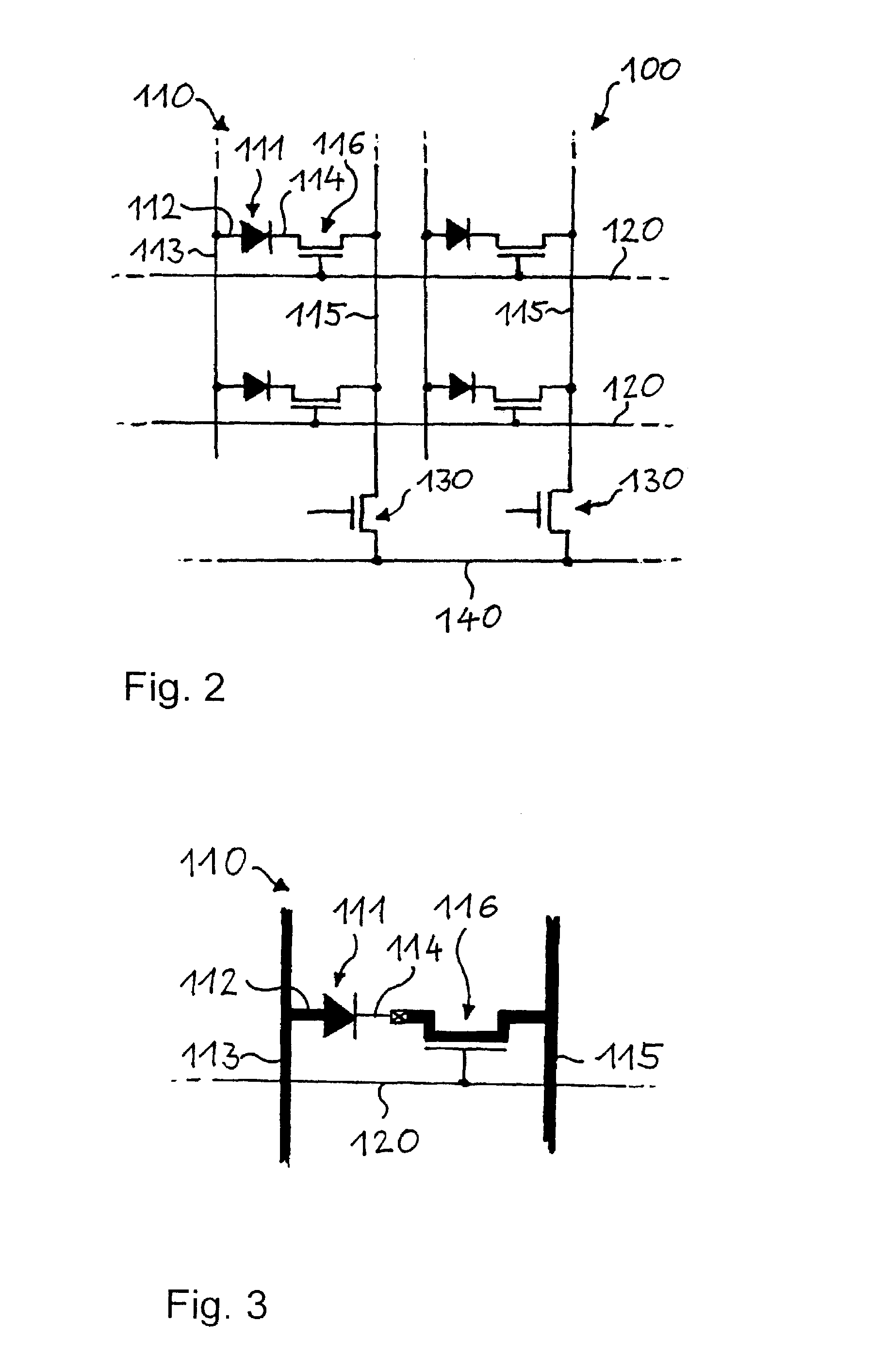
[0057]In an active-pixel-display unit cell 110, one terminal 112 of a light-emitting-diode (LED) structure 111 is connected to a fixed-voltage line 113, while the other terminal 114 is connected via a transistor switch 116 to a variable-voltage line 115, as schematically illustrated in FIG. 2. A two-dimensional array 100 of one or more of such LED / transistor unit cells 110 is provided with at least one row-select line 120 that is connected to all gates of the transistor switches 116 in a row. The transistor switches 116 of each row have their drain contacts connected to a column line 115. Each column line 115 is connected via a column-select transistor 130 to a common signal line 140.

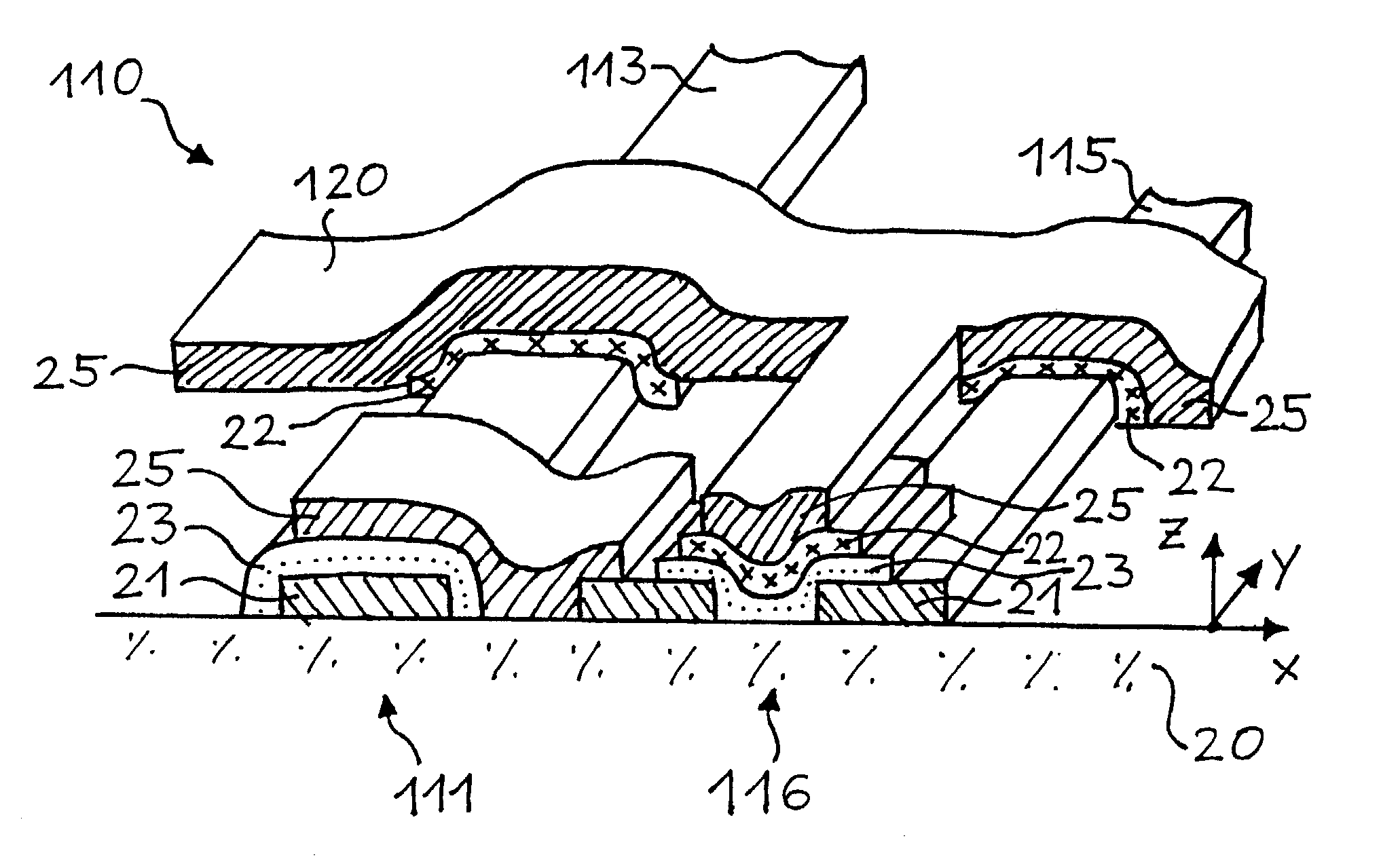
[0058]FIG. 3 shows a preferred realization of an active-pixel-LED-display unit cell 110, making use of the fabrication process explained with reference to FIG. 1. A preferred implementation of the same active-pixel-LED-display unit cell 110 is shown in a perspective view i...


PUM


Abstract

The monolithic integration of all key photonic components (11–16) of an integrated-optical microsystem (1) based on organic semiconductors is disclosed. Examples of such components (11–16) are light sources (11), photodetectors (12), photovoltaic power generators (12), field-effect transistors (13, 14), resistors, capacitors (15), or waveguiding structures (11, 12). The components (11–16) are arranged on a common substrate (20), are compatible with each other, can be manufactured simultaneously and can be operated simultaneously. At least one of the components (11–14) comprises a layer (23) of organic semiconductor material. Each component (11–16) comprises a plurality of layers (21–26), at least one of which (21) has identical physical and chemical characteristics in at least two components (11–16). The large number and diversity of photonic devices that can be monolithically integrated allows a higher degree of integration, of functionality and of system complexity than was practical with the state of the art.

Description

BACKGROUND OF THE INVENTION[0001]1. Field of the Invention[0002]This present invention generally relates to integrated-optical microsystems and, more particularly, to an integrated-optical microsystem based on organic semiconductors and to a method for manufacturing the same. An integrated-optical microsystem comprises at least two different electronic, photonic and / or micromechanic components arranged on a common substrate. Important examples of such components are monochromatic (laser) or polychromatic (LED) light sources, photodetectors, photovoltaic power generators, p-channel and n-channel field-effect transistors, resistors, capacitors, light-guiding or wave-guiding structures, or derived sensing devices for the measurement of pressure, magnetic or electric fields, chemical or bio-chemical substances, etc. Applications include self-powered posters or business cards, millimeter-thin large-area scanners and electronic paper.[0003]2. Description of Related Art[0004]Known techniqu...

Claims


Application Information

Patent Timeline
Patent Type & Authority Patents(United States)
IPC IPC(8): H01L35/24H01L27/00H01L27/146H01L31/0328
CPCH01L27/14627H01L27/14601
Inventor SEITZ, PETER
Owner CSEM CENT SUISSE DELECTRONIQUE & DE MICROTECHNIQUE SA RECH & DEV
Why Eureka
Try Eureka