Display device

a display device and display technology, applied in the field of display devices, can solve the problems of low reliability of conventional display devices, impaired reliability, and high probability of malfunction, and achieve the effect of high reliability of display devices

Active Publication Date: 2014-03-06
SEMICON ENERGY LAB CO LTD
View PDF2 Cites 33 Cited by
  • Summary
  • Abstract
  • Description
  • Claims
  • Application Information

AI Technical Summary

Benefits of technology

[0019]According to one embodiment of the present invention, a highly reliable display device can be provided. Further, a display device with a narrow frame can be provided.

Problems solved by technology

A conventional display device has a problem of low reliability.
However, entry of water or the like from the outside through the sealant into a sealed region degrades the characteristics of the display element or a transistor for driving the display element; thus, a malfunction is likely to occur.
Further, in the case where an EL element is used as the display element, there is a problem in that reliability is impaired by entry of impurities such as moisture and oxygen from the outside.

Method used


Image

  • Display device
  • Display device
  • Display device

Examples


embodiment 1

[0030]In this embodiment, a display device according to one embodiment of the present invention will be described with reference to FIGS. 1A and 1B, FIGS. 2A and 2B, and FIGS. 3A to 3C. In this specification and the like, a display device includes a light-emitting display device, a liquid crystal display device, and a display device including an electrophoretic element. A light-emitting display device includes a light-emitting element, and a liquid crystal display device includes a liquid crystal element. A light-emitting element includes, in its scope, an element whose luminance is controlled by current or voltage, and specifically includes an inorganic EL element, an organic EL element, and the like.

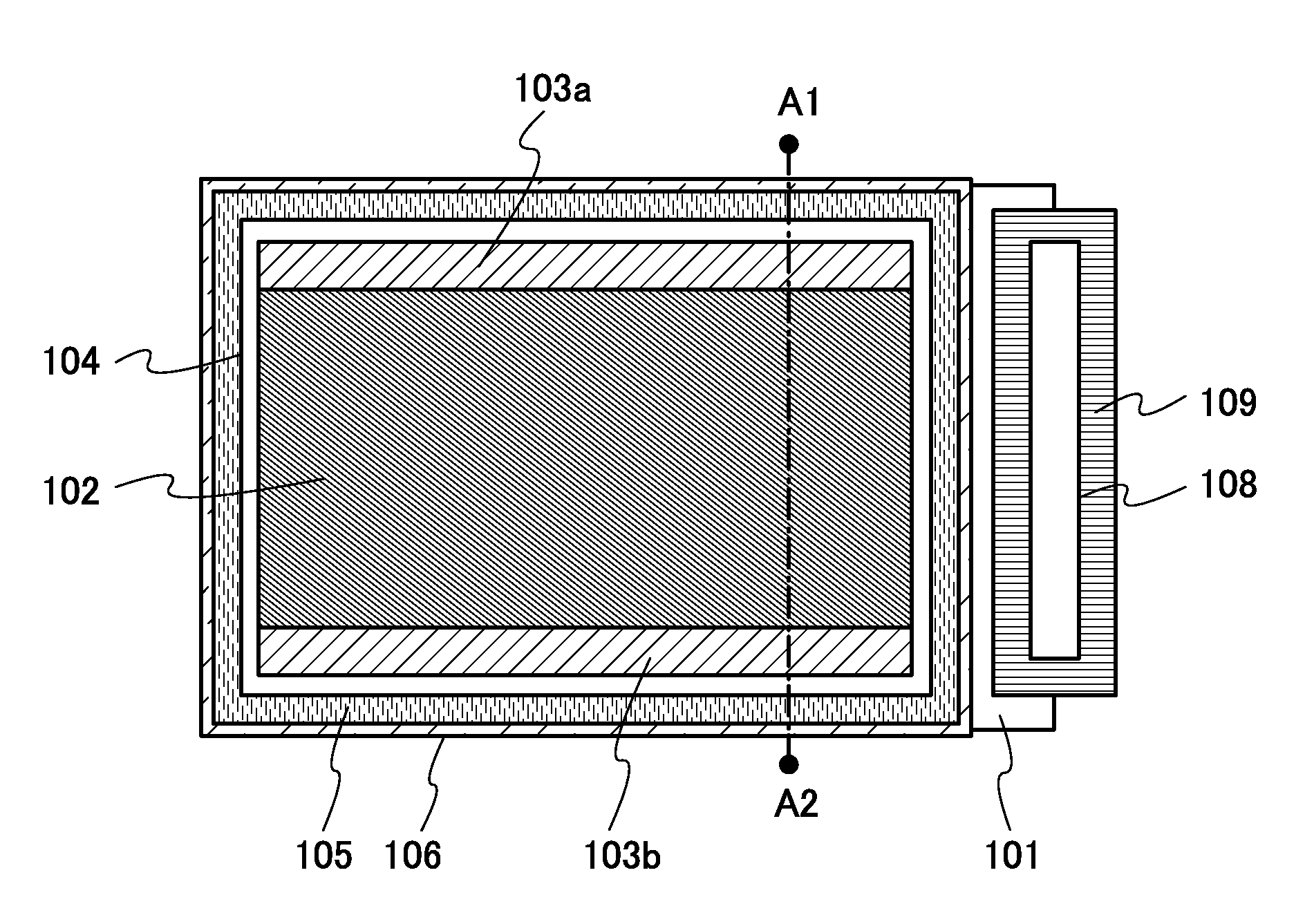
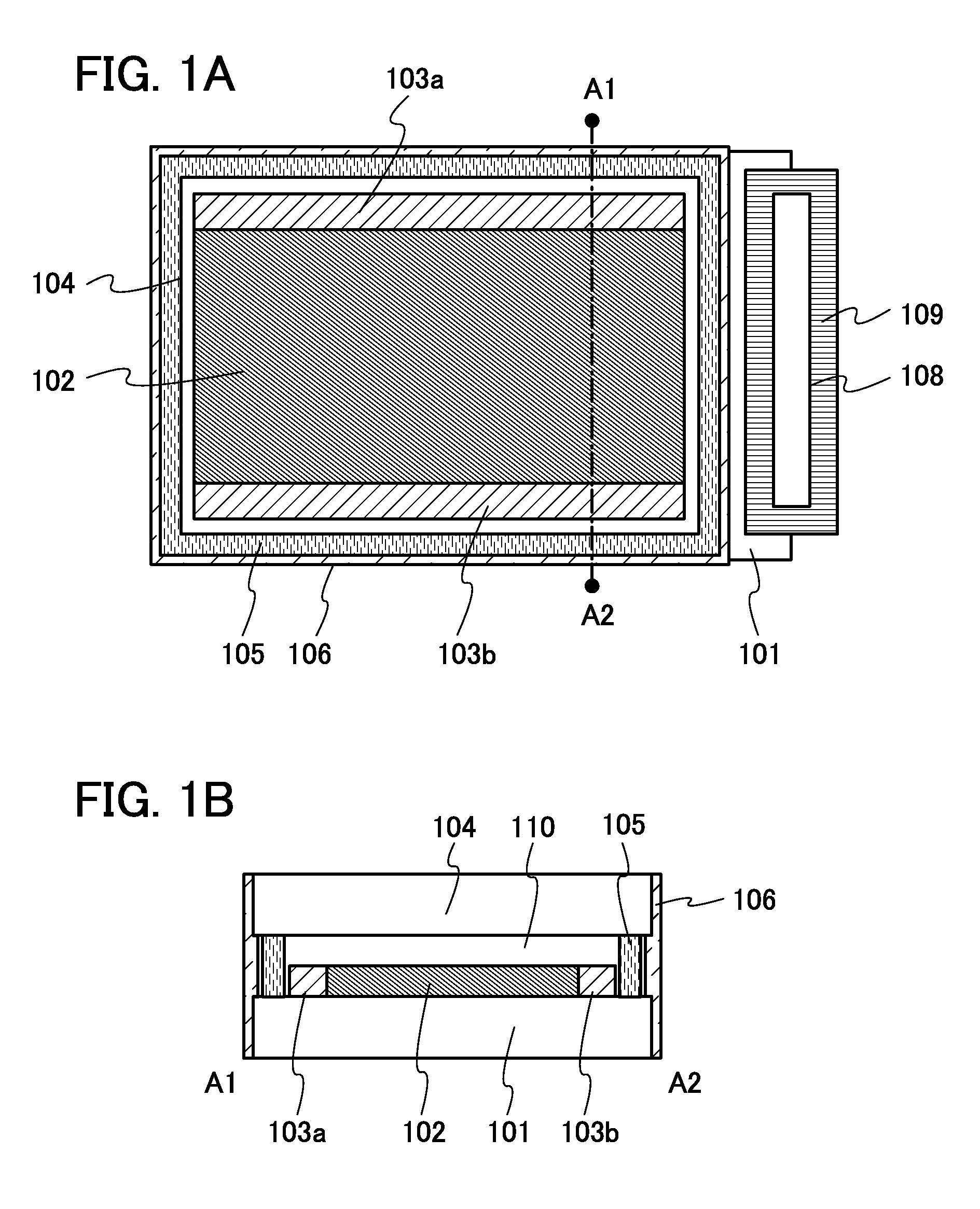
[0031]FIGS. 1A and 1B illustrate a display device according to one embodiment of the present invention. FIG. 1A is a top view of the display device, and FIG. 1B is a cross-sectional view taken along dashed-dotted line A1-A2 in FIG. 1A.

[0032]As illustrated in FIG. 1A, the display device...

embodiment 2

[0078]In this embodiment, a manufacturing method of a display device according to one embodiment of the present invention will be described with reference to FIGS. 4A1, 4A2, 4B1, 4B2, 4C1, and 4C2 and FIGS. 5A1, 5A2, 5B1, 5B2, 5C1, and 5C2. In particular, the display device illustrated in FIGS. 2A and 2B will be described as an example.

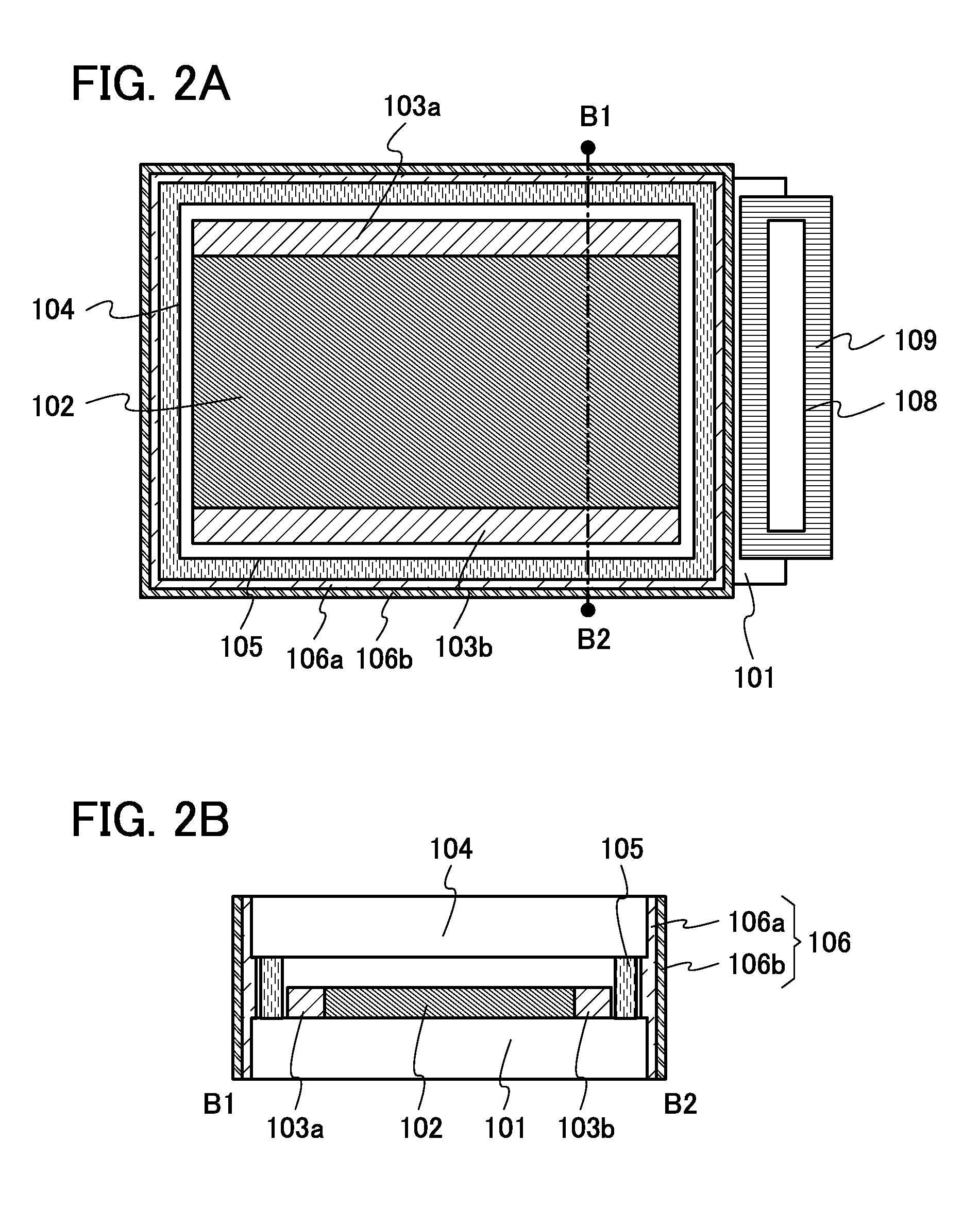
[0079]First, a manufacturing method of the third structural example of the display device illustrated in FIGS. 2A and 2B will be described with reference to FIGS. 4A1, 4A2, 4B1, 4B2, 4C1, and 4C2 and FIGS. 5A1, 5A2, 5B1, 5B2, 5C1, and 5C2. First, the pixel portion 102 and the driver circuit portions 103a and 103b are formed over the first substrate 101 (see FIGS. 4A1 and 4A2). Specifically, a display element in the pixel portion 102, and transistors in the driver circuit portions 103a and 103b such as a transistor controlling the display element are formed.

[0080]Next, the first sealant 105 is formed over the second substrate 104 (see FIGS. 4B1 and 4B2...

embodiment 3

[0106]In this embodiment, a light-emitting display device according to one embodiment of the present invention will be described with reference to FIGS. 6A and 6B.

[0107]FIGS. 6A and 6B illustrate a light-emitting display device according to one embodiment of the present invention. FIG. 6A is a top view of the light-emitting display device, and FIG. 6B is a cross-sectional view taken along dashed-dotted line B1-B2 in FIG. 6A.

[0108]In the active matrix light-emitting display device according to one embodiment of the present invention, a pixel portion 202 and scan line driver circuit portions 203a and 203b are provided between a first substrate 201 and a second substrate 204. A first sealant 205 is provided around the periphery of the pixel portion 202 and the scan line driver circuit portions 203a and 203b. A gap between the first substrate 201 and the second substrate 204 is filled with a second sealant 206a. The second sealant 206a is in contact with side surfaces of the first subst...


PUM


Abstract

A highly reliable display device is provided. Alternatively, a display device with a narrow frame is provided. The display device includes: a first substrate and a second substrate facing each other; a pixel portion including a display element, between the first substrate and the second substrate; a first sealant provided around a periphery of the pixel portion; a second sealant which is in contact with at least one of a side surface of the first substrate and a side surface of the second substrate and with which a gap between the first substrate and the second substrate is filled; and a third sealant overlapping with a side surface of the first sealant and at least one of the side surface of the first substrate and the side surface of the second substrate with the second sealant interposed therebetween.

Description

BACKGROUND OF THE INVENTION[0001]1. Field of the Invention[0002]The present invention relates to a display device and a manufacturing method thereof.[0003]2. Description of the Related Art[0004]In recent years, techniques for improvement in performance (e.g., reduction in power consumption or increase in definition) of a display device have been developed.[0005]Examples of the display device include a liquid crystal display device, an electroluminescent display device (also referred to as an EL display device), and the like.[0006]As a transistor for driving a display element (a liquid crystal element, an EL element, or the like) in the display device, a transistor in which a channel formation region includes a silicon semiconductor, a transistor in which a channel formation region includes a metal oxide semiconductor, or the like can be used. For example, a display device disclosed in Patent Document 1 is an example of a display device including, as a transistor for driving a displa...

Claims


Application Information

Patent Timeline
Patent Type & Authority Applications(United States)
IPC IPC(8): H01L51/52
CPCH01L51/5246H10K50/8426G09F9/00H01L33/56G09G3/3208H10K50/8423
Inventor YAMAZAKI, SHUNPEIHIRAKATA, YOSHIHARUNISHI, TAKESHI
Owner SEMICON ENERGY LAB CO LTD
Why Eureka
Try Eureka