Image display device

a display device and image technology, applied in the direction of discharge tube/lamp details, discharge tube/lamp details, incadescent body mounting/support, etc., can solve the problems of air leakage in the hermetically sealed portions, inability to secure safety from possible danger, etc., to reduce the amount of alignment errors, high precision, and high-quality image display

Active Publication Date: 2008-02-19
PANASONIC LIQUID CRYSTAL DISPLAY CO LTD +1
View PDF4 Cites 19 Cited by
  • Summary
  • Abstract
  • Description
  • Claims
  • Application Information

AI Technical Summary

Benefits of technology

[0010]There has been a problem with the image display device disclosed in the above-mentioned Japanese Patent No. 3,129,909 (Japanese Patent Application Laid-Open Publication No. Hei 7-302,540). Since the thickness H1 of the coated glass frit 10 for fixing the support frame 3 after being subjected to a preparatory firing is selected to be greater than the thickness H2 of the coated glass frit 11 for fixing the spacers 4 after being subjected to a preparatory firing, the spacers 4 do not touch the glass frits 11 until the glass frit 10 is melted for assembling the display panel, and consequently, the spacers 4 are easily tilted and as a result errors occur easily in aligning of the front and rear plates.
[0016]Therefore the present invention has been made to solve the above-explained problems with the conventional image display devices, and it is an object of the present invention to provide an image display device capable of producing a high-quality image display by reducing the amount of alignment errors in sealing of the front and rear planes.
[0017]It is another object of the present invention to provide an image display device capable of producing a highly reliable image display by dispersing the force of atmospheric pressure applied approximately uniformly over the entirety of the display panel comprised of the front and rear substrates, the support member, and the spacing-maintaining members, and thereby preventing tilt and breakage of the spacing-maintaining members.
[0034]In the present invention, by selecting the height of the spacing-maintaining members to be greater than the height of the support member, the spacing between the front and rear substrates is determined by the height of the spacing-maintaining members, resulting in reduction of the amount of alignment errors in sealing of the support member disposed between the front and rear substrates, therefore the spacing between the front and rear substrates is controlled to be held uniform with high precision, and consequently, the present invention provides extremely great advantages such as the realization of producing a high-quality image display.
[0035]Further, in the present invention, the rear substrate and one end face of the support member are bonded together hermetically with a first sealing member interposed therebetween, and the front substrate and the other end face of the support member are bonded together hermetically with a second sealing member interposed therebetween, therefore the spacing between the front and rear substrates is held securely, and at the same time damage to the spacing-maintaining members and attendant damage to electrodes and others can be prevented. Consequently, the present invention provides extremely great advantages such as the realization of producing a highly reliable image display.
[0036]Further, in the present invention, since the force of atmospheric pressure is dispersed approximately uniformly over the entire area of the display panel comprised of the front and rear substrates, the support member, and the spacing-maintaining members, the spacing-maintaining members are prevented from being tilted and others, thereby improving greatly the safety from possible danger caused by atmospheric pressure, such as resistance to implosion. Consequently, the present invention provides the present invention provides the extremely great advantages such as the realization of producing a highly reliable image display.

Problems solved by technology

There has been a problem with the image display device disclosed in the above-mentioned Japanese Patent No. 3,129,909 (Japanese Patent Application Laid-Open Publication No.
Also there has been a problem with the image display device disclosed in the above-mentioned Japanese Patent No. 3,241,219 (Japanese Patent Application Laid-Open Publication No.
Consequently, the force of atmospheric pressure is not applied uniformly all of the spacers 4, and it was not possible to secure safety from possible danger caused by atmospheric pressure, such as resistance to implosion.
Hei 7-230,776, which corresponds to U.S. Pat. No. 5,734,224), it is very difficult to fix the spacers 4 disposed in a display area between the front plate 1 and the rear substrate 2, without occurrences of alignment errors or tilts, there is also a problem in that the spacers 4 are broken, and the broken spacers 4 damage electron-emissive elements 5 and electrodes, and there is also a danger that the addition of the process of bonding the spacers 4 causes cracks and air leakage in the hermetically sealed portions.

Method used


Image

  • Image display device
  • Image display device
  • Image display device

Examples


embodiment 1

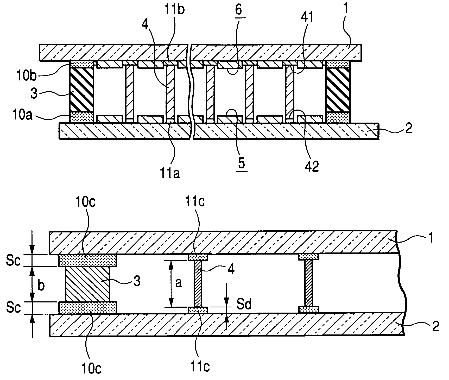
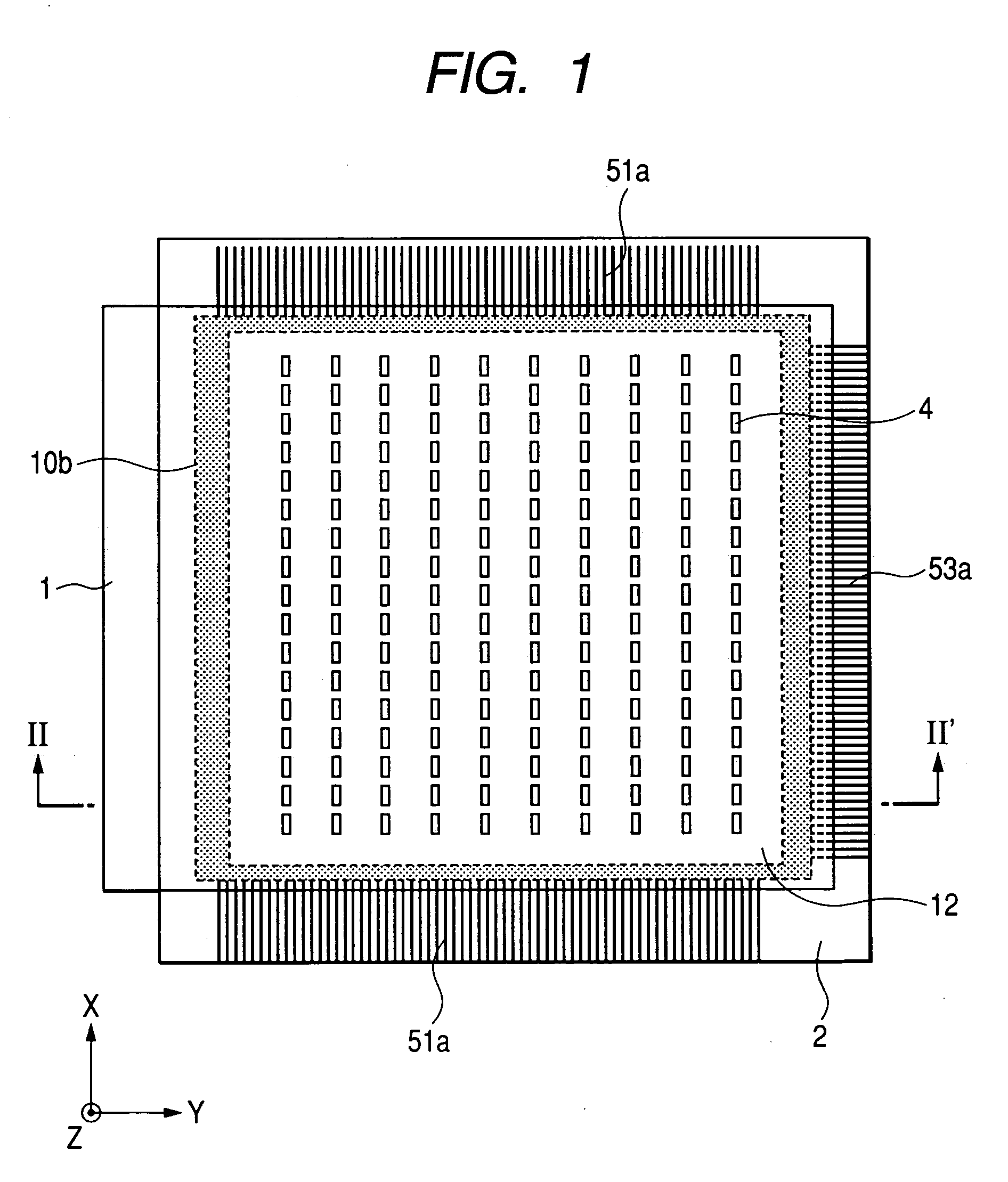
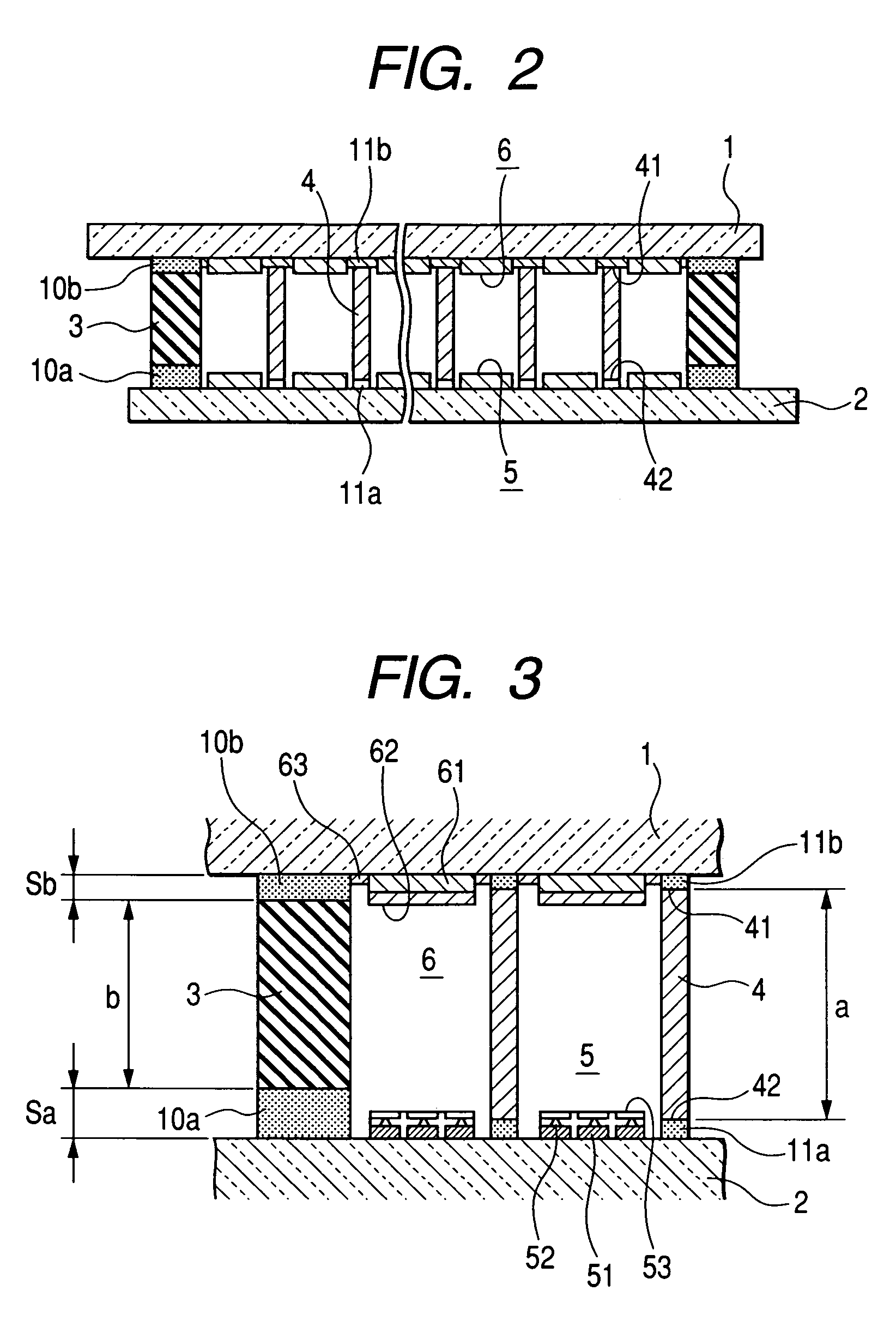
[0051]FIG. 1 is a plan view of a major portion of an electron-emission type display device in accordance with Embodiment 1 of the image display device of the present invention for explaining the rough configuration of the electron-emission type display device, FIG. 2 is an enlarged cross-sectional view of the major portion of the electron-emission type display device of FIG. 1 taken along line II-II′ of FIG. 1, and FIG. 3 is an enlarged cross-sectional view of a major portion of the electron-emission type display device of FIG. 2. In FIGS. 1 to 3, reference numeral 1 denotes a front substrate comprised of light-transmissive glass plate, 2 is a rear substrate comprised of a light-transmissive glass plate as in the case of the front substrate 1, or comprised of a ceramic plate such as an alumina plate. The front and rear substrates 1, 2 are comprised of insulating substrates of about 3 mm in thickness, for example. Reference numeral 3 denotes a support frame which is a supporting memb...

embodiment 2

[0081]In this Embodiment of the image display device in accordance with the present invention, in a case where the sealing thickness Sa of the sealing member 10a is selected to be greater than the sealing thickness Sb of the sealing member 10b, the material of the sealing member 10a for bonding the support frame 3 to the rear substrate 2 is made different from that of the sealing member 10b for bonding the support frame 3 to the front substrate 1. FIG. 12 tabulates some examples of combinations of sealing members comprised of materials different from each other.

[0082]As an example of the silicone adhesives in FIG. 12, there is a silicone resin adhesive comprising at least phenylheptamethylcyclotetrasiloxane and 2,6-cis-diphenylhexamethylcyclotetrasiloxane, which is an adhesive capable of maintaining hermetic sealing performance at high temperatures, proposed by Japanese Patent Application Laid-Open Publication No. 2,004-182,959.

[0083]The constituent material of the sealing member 10...

embodiment 3

[0085]FIG. 6 is a cross-sectional view of a major portion of an electron-emission type display device in accordance with Embodiment 3 of the image display device of the present invention for explaining the rough configuration of the electron-emission type display device, the same reference numerals as utilized in the above-explained figures designate corresponding portions in FIG. 6, and the explanation of those portions is omitted.

[0086]Omitted in FIG. 6 are the details of the electron-emissive elements 5 formed on the inner surface of the rear substrate 2 and the image-forming members 6 formed on the inner surface of the front surface 1. Since the spacers 4 are usually fabricated by cutting a thin glass plate or a thin ceramic plate such as an alumina plate into small-piece components, the spacers 4 can be fabricated with their height a being held to close tolerances. As shown in an enlarged cross-sectional view of the major portion of the image display device, if the spacing betw...


PUM


Abstract

An image display device has a front substrate having an anode and phosphors, a rear substrate having electron sources and opposing the front substrate with a specified spacing therebetween, a support member which is sandwiched between the front and rear substrates, surrounds a display region, and maintains the specified spacing, and plural spacing-maintaining members which are sandwiched between the front and rear substrates in the display region, and are fixed at at least one of end faces of each of the spacing-maintaining members to a corresponding one of the front and rear substrates. Both end faces of the support member is hermetically sealed to the rear and front substrates, respectively. A height of the spacing-maintaining members is greater than that of the support member.

Description

CLAIM OF PRIORITY[0001]The present application claims priority from Japanese application serial no. 2004-307728, filed on Oct. 22, 2004, the content of which is hereby incorporated by reference into this application.BACKGROUND OF THE INVENTION[0002]The present invention relates to an image display device which utilizes emission of electrons into a vacuum produced between a front substrate and a rear substrate, and in particular to a configuration of a combination of a support-member and spacing-maintaining members which support and seal the front and rear substrates with a desired spacing therebetween.[0003]Conventionally, color cathode ray tubes have been widely used as display devices excellent in producing high-brightness high-definition display devices. However, as the image quality in information processing equipment and TV broadcasts has been improved in recent years, the demand has been becoming stronger for flat panel display devices capable of realizing lighter weight and t...

Claims


Application Information

Patent Timeline
Patent Type & Authority Patents(United States)
IPC IPC(8): H01J1/62
CPCH01J29/86H01J29/864H01J31/123H01J2211/48H01J2329/8625
Inventor KIJIMA, YUUICHIHIRASAWA, SHIGEMIKATO, KENJIHATORI, AKIRA
Owner PANASONIC LIQUID CRYSTAL DISPLAY CO LTD
Why Eureka
Try Eureka