Power Supply Device and Display Device
a technology of power supply device and display device, which is applied in the direction of transformer/inductance details, transformer/react mounting/support/suspension, electrical apparatus construction details, etc., can solve the disadvantages of transformer and switching element disadvantageously easily malfunctioning, heat generated by transformer and switching element disadvantageously easily transferred to the switching element,
- Summary
- Abstract
- Description
- Claims
- Application Information
AI Technical Summary
Benefits of technology
Problems solved by technology
Method used
Image
Examples
first embodiment
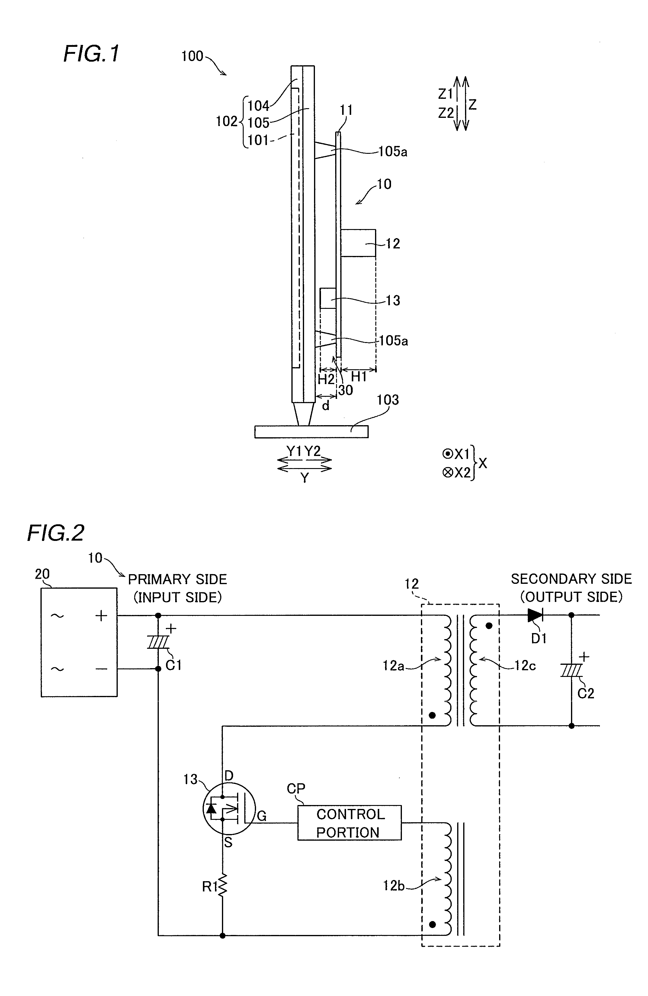
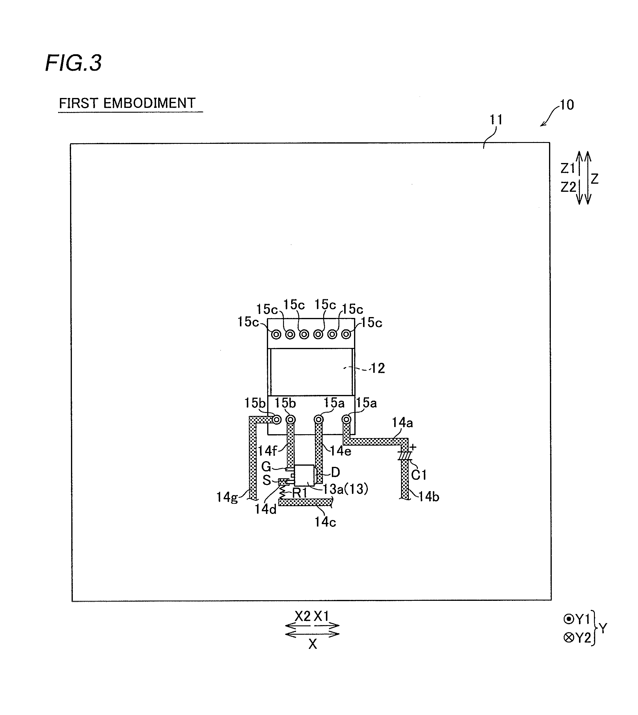
[0040]The structure of a display device 100 employing a power supply device 10 according to a first embodiment of the present invention is now described with reference to FIGS. 1 to 4. The power supply device 10 is an example of the “power supply portion” in the present invention.
[0041]As shown in FIG. 1, the display device 100 includes a display device body 102 including a display portion 101 displaying an image and a support member 103 supporting the display device body 102 from below (arrow Z2 direction side). The display device 100 is set perpendicularly to a horizontal plane (a plane extending in a direction X and a direction Y).
[0042]The display device body 102 of the display device 100 includes the display portion 101, a front housing 104 of resin holding the display portion 101 from the front surface side (arrow Y1 direction side), and a rear housing 105 of sheet metal holding the display portion 101 from the rear surface side (arrow Y2 direction side). The rear housing 105 ...
second embodiment
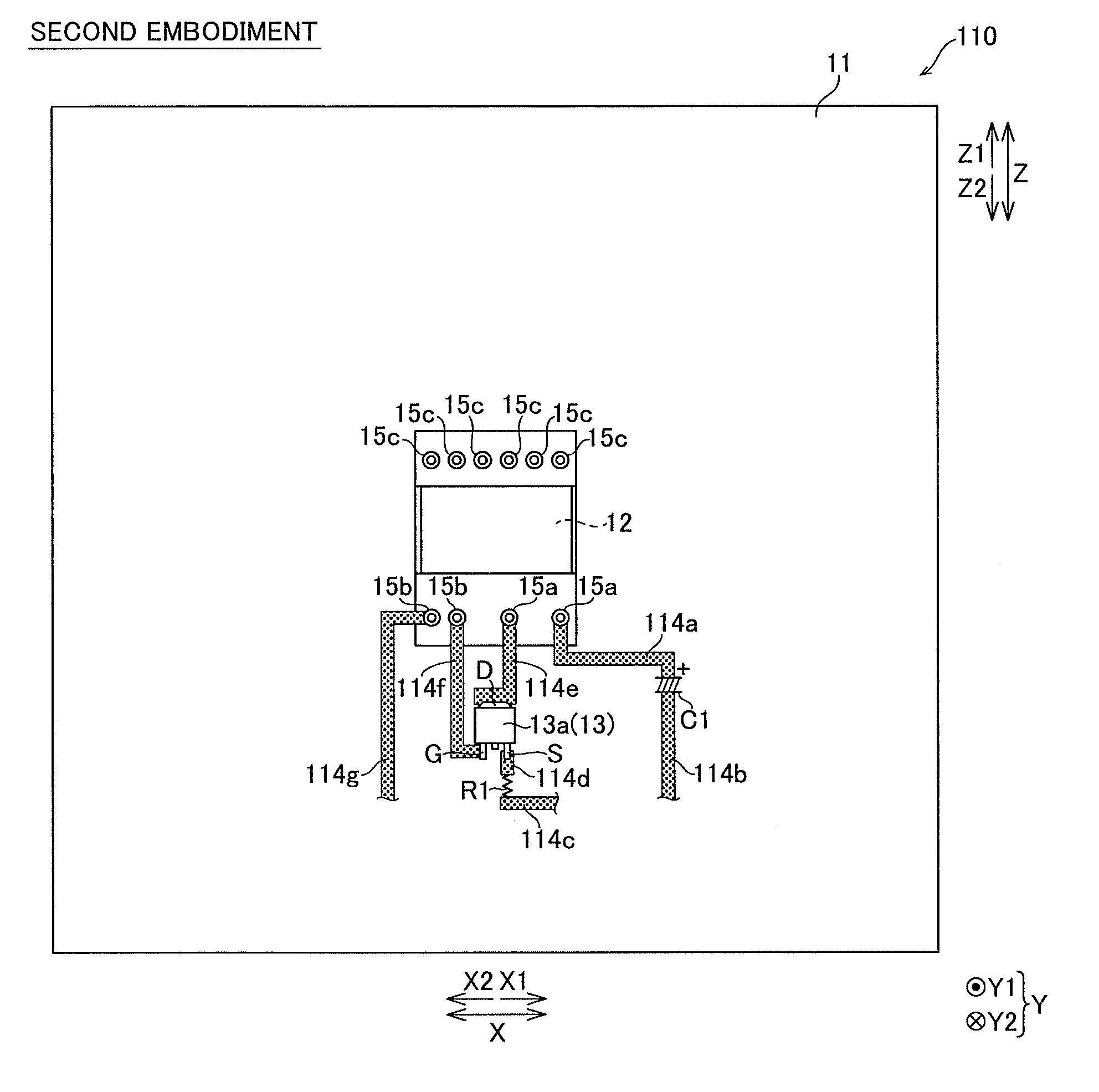
[0075]A power supply device 110 according to a second embodiment is now described with reference to FIGS. 5 and 6. In this second embodiment, the drain terminal D of an FET 13 is arranged to face to the side of a transformer 12 (upper side: arrow Z1 direction side), unlike in the aforementioned first embodiment in which the drain terminal D of the FET 13 is arranged to face to the side of the connection terminal portions 15a (right side: arrow X1 direction side).
[0076]As shown in FIG. 5, also in the second embodiment, connection terminal portions 15a and 15b connected to the transformer 12 mounted on the front surface (the surface on the arrow Y2 direction side) of a substrate 11 are provided on the rear surface (the surface on the arrow Y1 direction side) of the substrate 11, like in the aforementioned first embodiment. These connection terminal portions 15a and 15b are arranged on the right side (arrow X1 direction side) and the left side (arrow X2 direction side), respectively, a...
PUM
 Abstract
Description
Claims
Application Information


