

Nanocrystal display
a technology of nano-crystals and display devices, applied in non-linear optics, instruments, optics, etc., can solve the problems of increased manufacturing costs complex manufacturing processes of liquid crystal display devices, etc., and achieve the effect of stabilizing the arrangement of liquid crystal molecules and reducing or effectively preventing the application of data signals
- Summary
- Abstract
- Description
- Claims
- Application Information
AI Technical Summary
Benefits of technology
Problems solved by technology
Method used
Image

Examples
Embodiment Construction
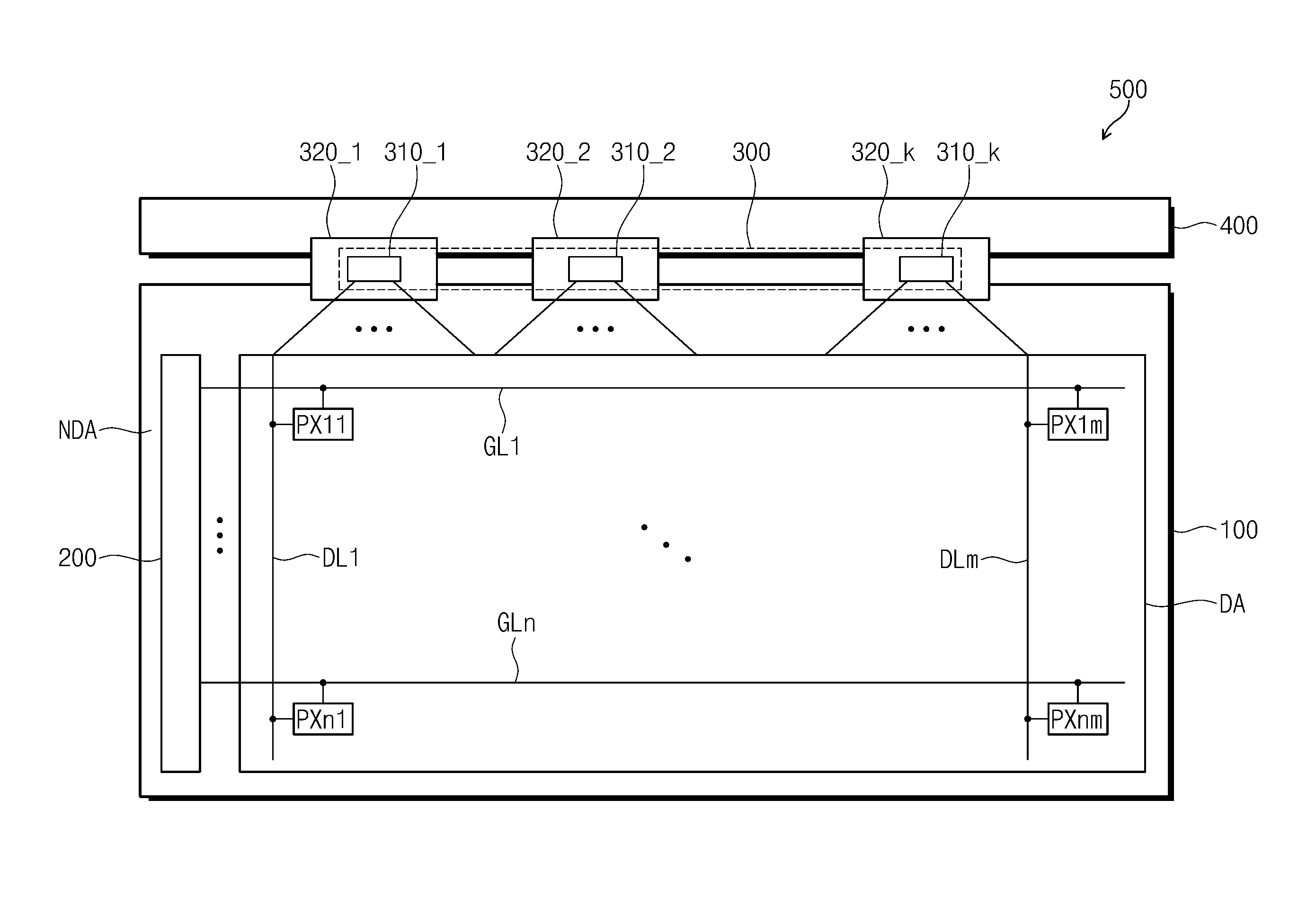
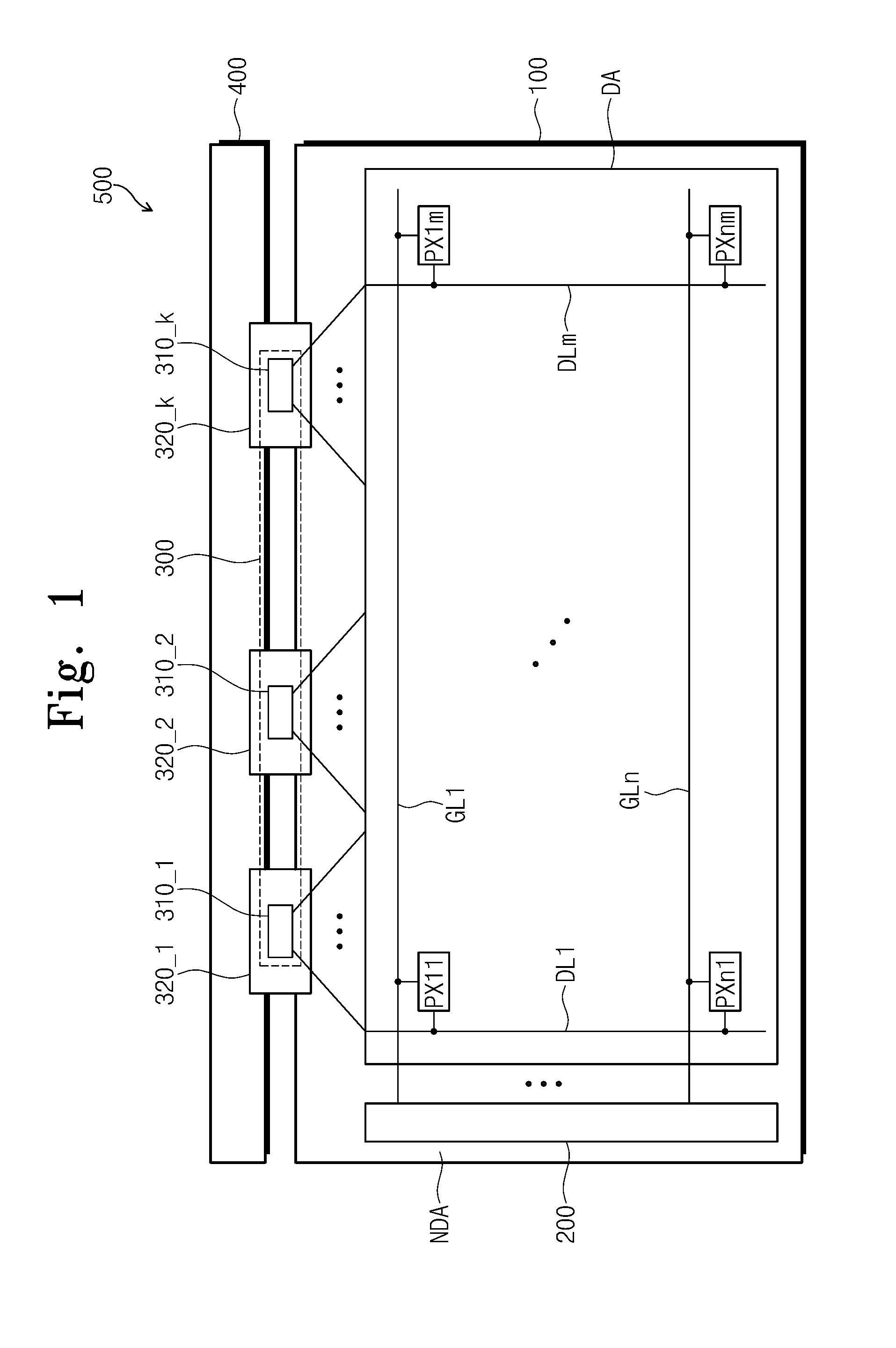
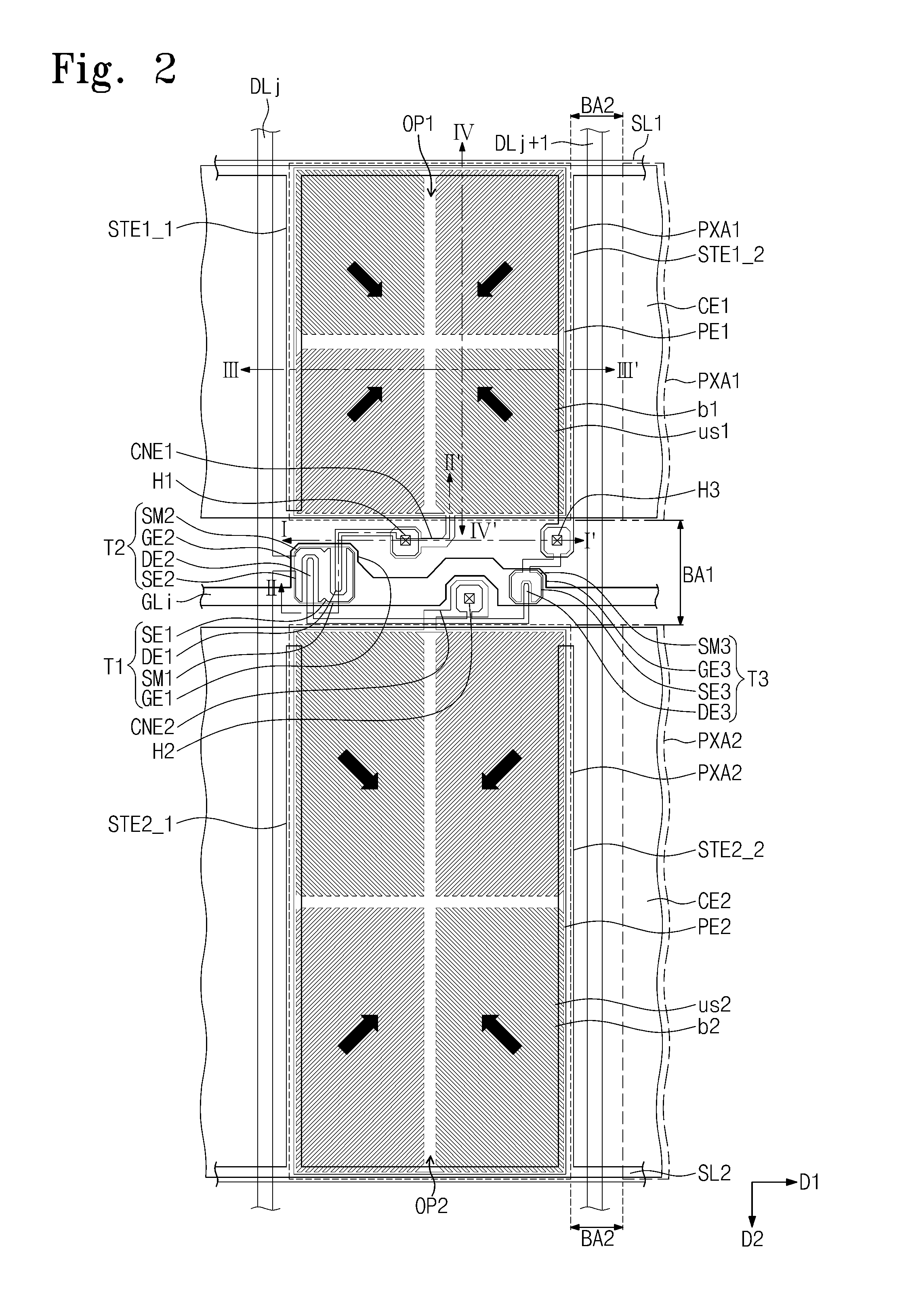
[0035]It will be understood that when an element or layer is referred to as being “on,” or “connected to” another element or layer, it can be directly on or connected to the other element or layer or intervening elements or layers may be present. In contrast, when an element is referred to as being “directly on” or “directly connected to” another element or layer, there are no intervening elements or layers present. As used herein, connected may refer to elements being physically and / or electrically connected to each other. Like numbers refer to like elements throughout. As used herein, the term “and / or” includes any and all combinations of one or more of the associated listed items.
[0036]It will be understood that, although the terms first, second, etc. may be used herein to describe various elements, components, regions, layers and / or sections, these elements, components, regions, layers and / or sections should not be limited by these terms. These terms are only used to distinguish...
PUM
| Property | Measurement | Unit |
|---|---|---|
| DA | aaaaa | aaaaa |
| area | aaaaa | aaaaa |
| areas | aaaaa | aaaaa |
Abstract
Description
Claims
Application Information