Charge and discharge control circuit and battery device
- Summary
- Abstract
- Description
- Claims
- Application Information
AI Technical Summary
Benefits of technology
Problems solved by technology
Method used
Image

Examples
first embodiment
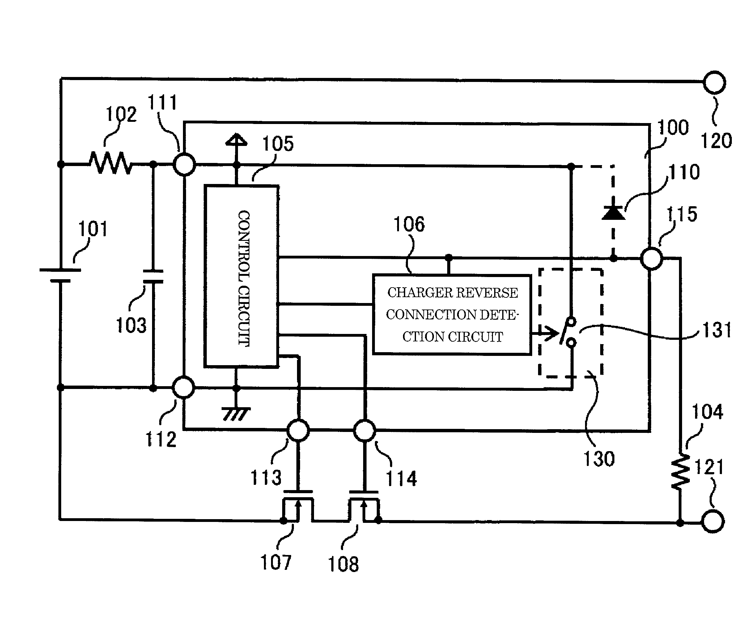
[0020]FIG. 1 is a circuit diagram of a charge and discharge control circuit and a battery device according to a first embodiment of the present invention.
[0021]The charge and discharge control circuit and the battery device according to the first embodiment include a secondary battery 101, resistors 102 and 104, a capacitor 103, a discharge control N-channel FET transistor 107, a charge control N-channel FET transistor 108, a charge and discharge control circuit 100, and external terminals 120 and 121. The charge and discharge control circuit 100 includes a control circuit 105, a charger reverse connection detection circuit 106, a consumption current increase circuit 130, a VDD terminal 111, a VSS terminal 112, a DO terminal 113, a CO terminal 114, and a VM terminal 115. The consumption current increase circuit 130 includes a switch circuit 131.
[0022]The secondary battery 101 has a positive terminal connected to the external terminal 120 and one terminal of the resistor 102, and a n...
second embodiment
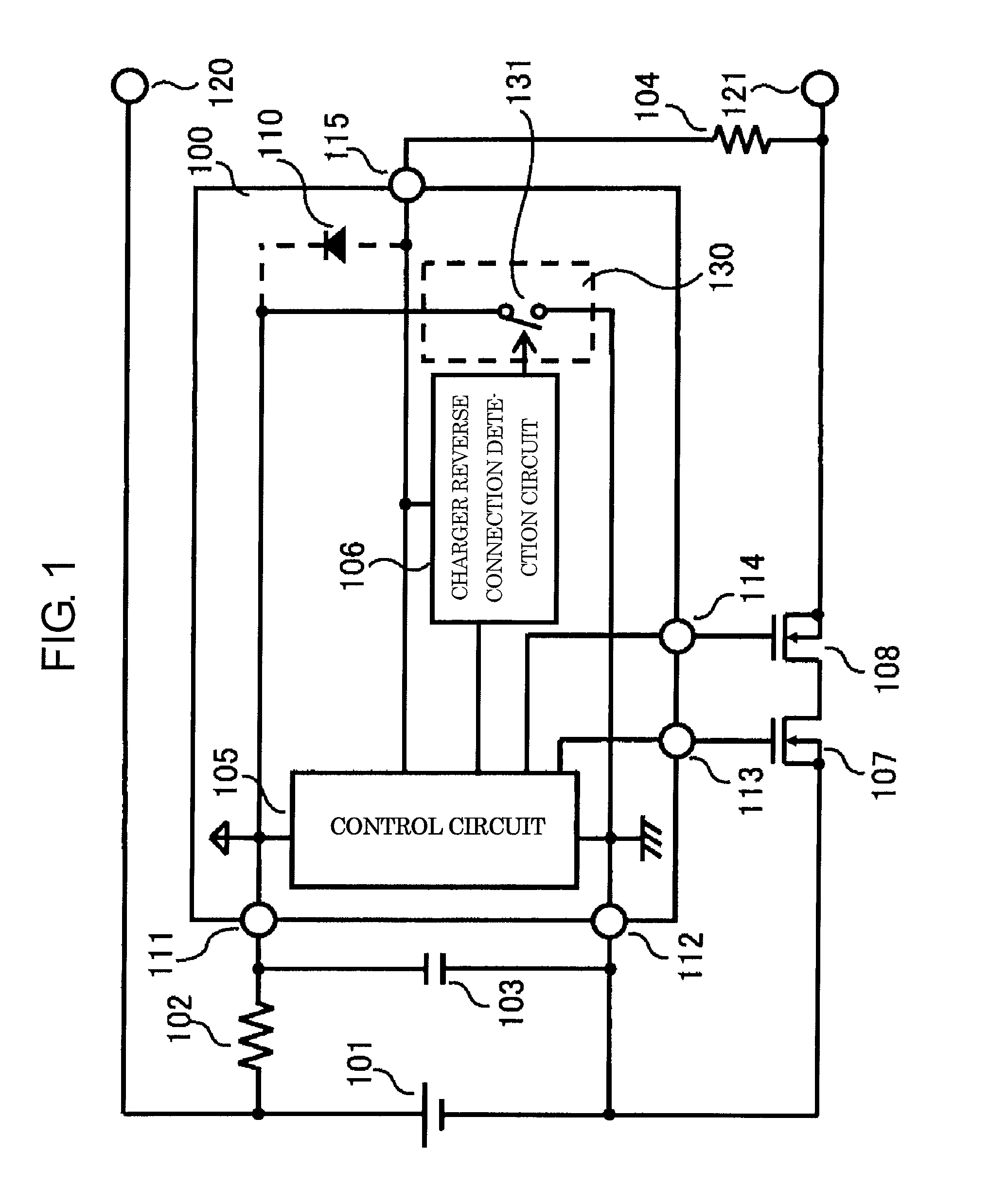
[0033]FIG. 2 is a circuit diagram of a charge and discharge control circuit and a battery device according to a second embodiment of the present invention.
[0034]The second embodiment differs from the first embodiment in that a resistor 201 as an impedance element is inserted between the switch circuit 131 and the VDD terminal 111. The rest is the same as in the first embodiment.
[0035]Operations of the charge and discharge control circuit and the battery device according to the second embodiment are described below.
[0036]Operations in the overcharge state, the overdischarge state, and the overcurrent state and an operation of the charger reverse connection detection circuit 106 are the same as those in the first embodiment. When entering the charger reverse connection state, the charger reverse connection detection circuit 106 turns on the switch circuit 131 to operate the consumption current increase circuit 130. Then, a current value Ids flows from the VDD terminal 111 to the VSS t...
third embodiment
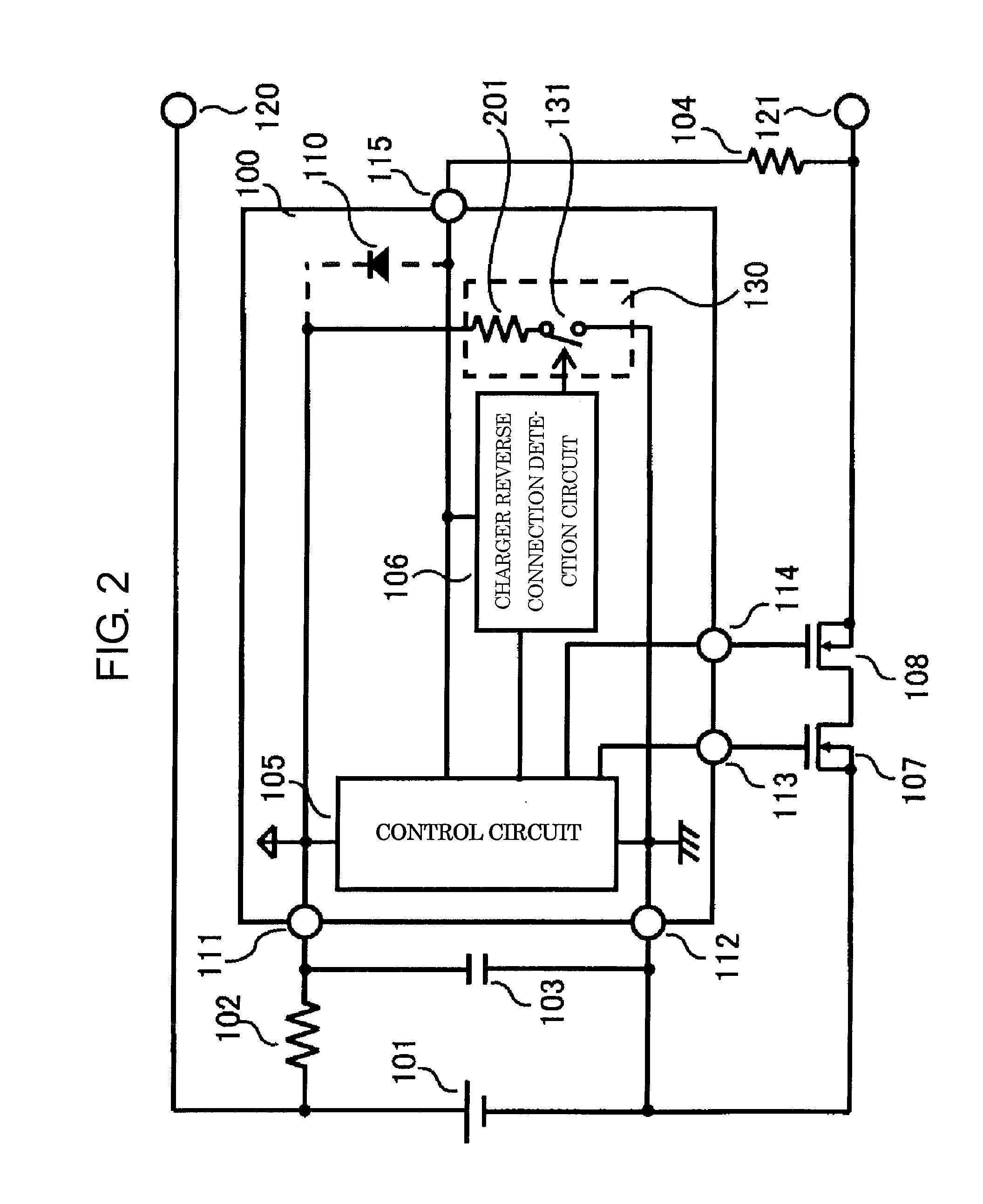
[0039]FIG. 3 is a circuit diagram of a charge and discharge control circuit and a battery device according to a third embodiment of the present invention.
[0040]The third embodiment differs from the second embodiment in that the resistor 201 is replaced by a constant current circuit 301. The rest is the same as in the second embodiment.
[0041]Operations of the charge and discharge control circuit and the battery device according to the third embodiment are described below.
[0042]Operations in the overcharge state, the overdischarge state, and the overcurrent state and an operation of the charger reverse connection detection circuit 106 are the same as those in the second embodiment. When entering the charger reverse connection state, the charger reverse connection detection circuit 106 turns on the switch circuit 131 to operate the consumption current increase circuit 130. Then, a current value Ids flows from the VDD terminal 111 to the VSS terminal 112. By adjusting the current Ids by...
PUM
 Abstract
Description
Claims
Application Information