
Semiconductor device having finfet structures and method of making same

a technology of semiconductor and fin, which is applied in the direction of semiconductor devices, basic electric elements, electrical equipment, etc., can solve the problem of difficult control of the width of the fin of each channel typ

Active Publication Date: 2014-09-11
RENESAS ELECTRONICS CORP
View PDF20 Cites 40 Cited by
  • Summary
  • Abstract
  • Description
  • Claims
  • Application Information

AI Technical Summary

Benefits of technology

The present invention relates to a method of making a semiconductor device and a semiconductor device comprising pFET and nFET transistors. The method involves depositing a layer of SiGe on a silicon layer and selectively etching the SiGe to form first fins with a stacked SiGe / Si structure. A second insulating layer is then formed to cover the first fins. The upper SiGe portions of the first fins are removed to expose the lower Si portions. A second silicon layer is then formed over the exposed lower Si portions to form second fins with an Si structure. The semiconductor device comprises pFET and nFET transistors with three-dimensional channel regions that overlie elevated regions of the insulating layer. The invention allows for improved performance and efficiency of semiconductor devices.

Problems solved by technology

However, with this technique, the width of the fins of each channel type is difficult to control relative to the other channel type, and may vary significantly.

Method used


Image

  • Semiconductor device having finfet structures and method of making same
  • Semiconductor device having finfet structures and method of making same
  • Semiconductor device having finfet structures and method of making same

Examples


Embodiment Construction

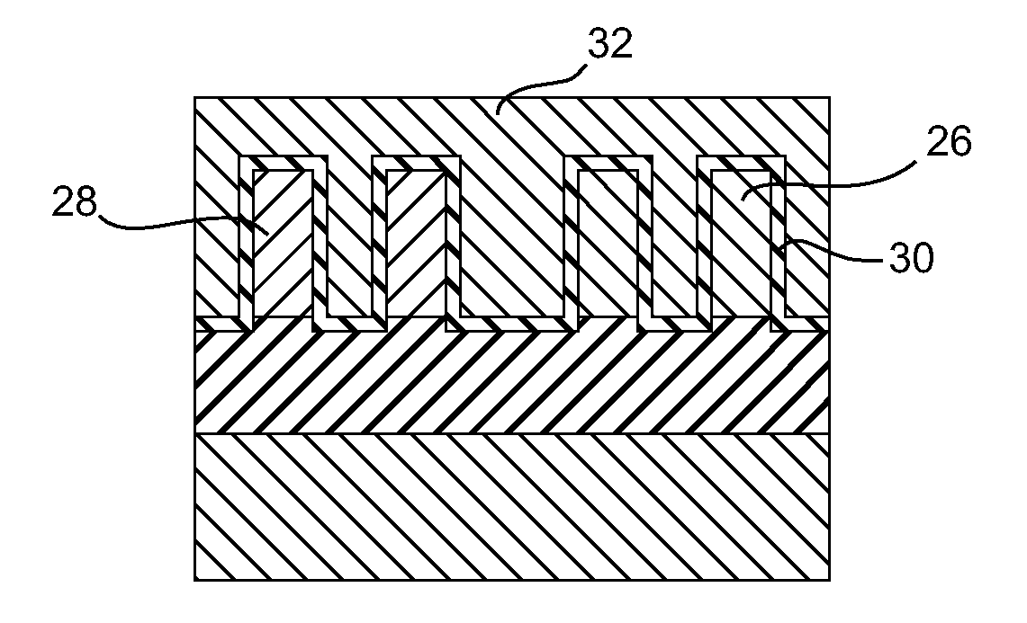
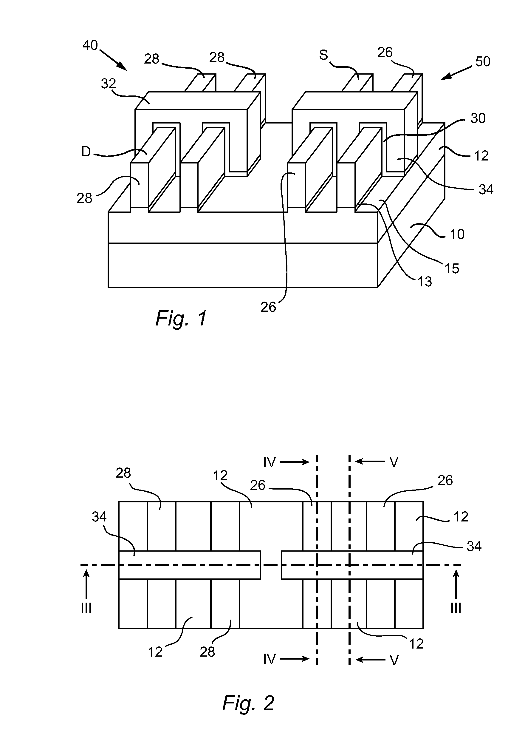
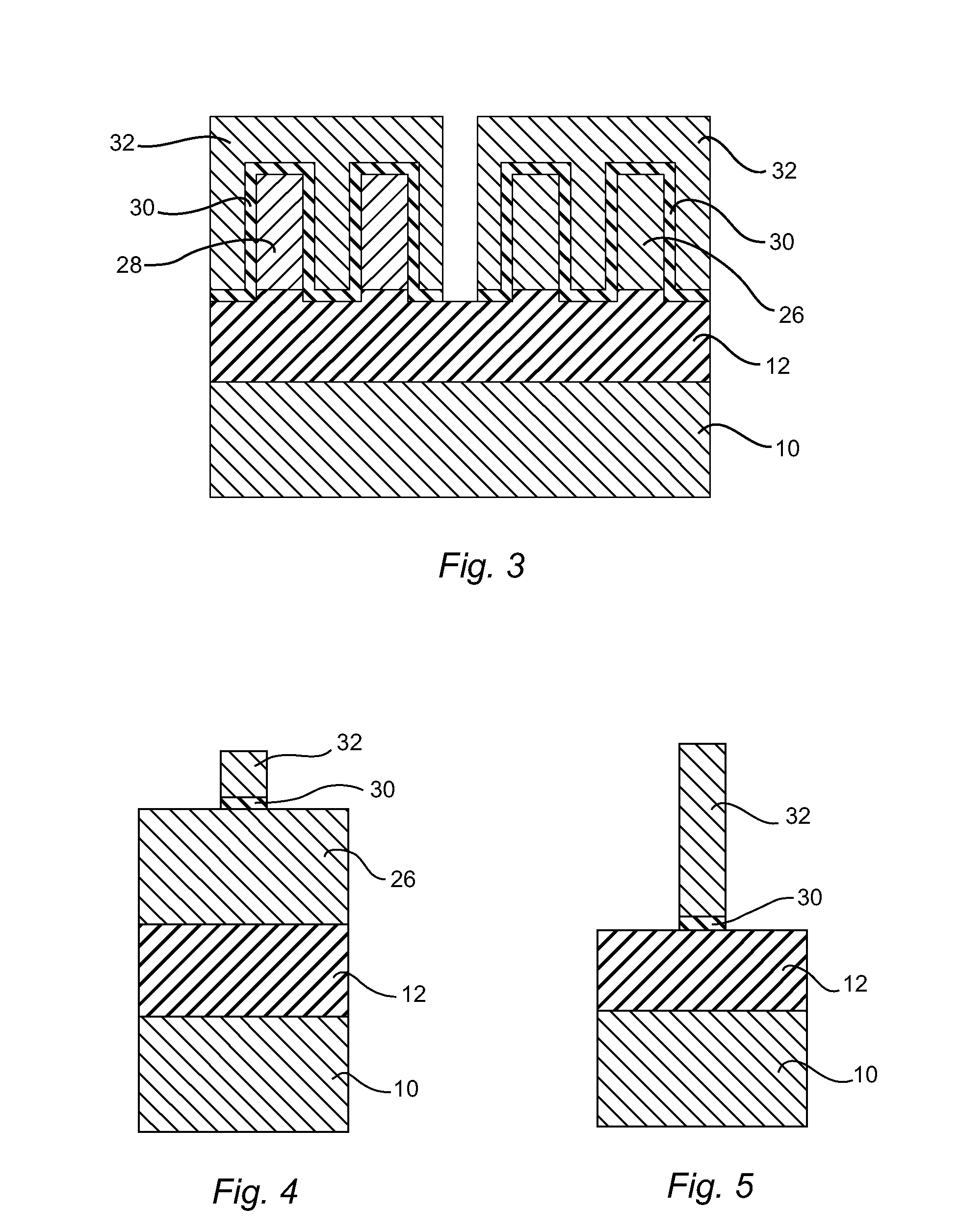
[0051]In FIGS. 1-5, a first embodiment of the present invention is a CMOS type semiconductor device that includes pFETs and nFETs, with an exemplary pFET being designated 40 and an exemplary nFET being designated 50. The device of FIG. 1 has been built on a silicon-on-insulator or SOI substrate, of which, in the finished device, the bulk silicon substrate 10 and the (initially buried) oxide layer 12 remain.

[0052]As can be seen in FIG. 1, the pFET 40 comprises a pair of fins 28, whereas the nFET 50 comprises a pair of fins 26. Fins 26, 28 project upwardly from the insulating layer 12, and overlie regions 13 of insulating layer 12 that are elevated in relation to surrounding regions 15 of the incubating layer 12. Each of pFET 40 and nFET 50 comprises a gate 32, for example made of polysilicon, which surrounds each of a respective pair of fins 26, 28 on three sides. A gate oxide layer 30 is formed between the gates 32 and their respective fins 26 or 28.

[0053]This configuration is also ...


PUM


Abstract

A semiconductor device and method making it comprises pFETs with an SiGe channel and nFETs with an Si channel, formed on an SOI substrate. Improved uniformity of fin height and width is attained by forming the fins additively by depositing an SiGe layer on the SOI substrate and forming first fins from the superposed SiGe layer and underlying thin Si film of the SOI substrate. Second fins of Si can then be formed by replacing the upper SiGe portions of selected first fins with Si.

Description

BACKGROUND OF THE INVENTION[0001]1. Field of the Invention[0002]The invention relates to semiconductor devices and methods of making the same, and more particularly relates to such devices and methods in which FinFET structures are formed on a semiconductor substrate.[0003]2. Description of Related Art[0004]As the gate length of transistors continues to decrease with successive generations of semiconductor devices, new transistor configurations have been needed to counteract the diminished response that would otherwise occur with shrinking gate lengths. One such design configuration is referred to variously as a FinFET or tri-gate transistor, in which the source, drain and channel region of each transistor is elevated relative to a semiconductor substrate. The elevated portion has the shape of a ridge or fin, and may be formed integrally with the underlying substrate or may be formed on an insulating layer in the case of SOI type devices. The gate wraps around the three projecting s...

Claims


Application Information

Patent Timeline
IPC IPC(8): H01L27/12H01L21/84
CPCH01L21/845H01L27/1211
Inventor NAGUMO, TOSHIHARU
Owner RENESAS ELECTRONICS CORP
Learn More