Capacitive in-cell touch screen panel and display device

a touch screen panel and capacitive in-cell technology, applied in the field of capacitive in-cell touch screen panel and display device, can solve the problems of high manufacturing cost, low light transmission ratio, and large thickness of modules

Inactive Publication Date: 2015-01-29
BEIJING BOE OPTOELECTRONCIS TECH CO LTD +1
View PDF30 Cites 25 Cited by
  • Summary
  • Abstract
  • Description
  • Claims
  • Application Information

AI Technical Summary

Benefits of technology

[0057]With the capacitive in-cell touch screen panel and the display device provided in the embodiments of the present invention, first touch detecting electrodes and second touch detecting electrodes insulated with each other are provided on a substrate; the first touch detecting electrodes are located between the substrate and the black matrix, the second touch detecting electrodes are located on a side of the black matrix away from the substrate. Because the first touch detecting electrodes and the second touch detecting electrodes are provided on the substrate away from the TFT array substrate, it is possible to avoid mutual interference between touch signals and display signals in the TFT array substrate, thereby not only ensuring the quality of pictures on a liquid crystal display but also enhancing reliability of touch operations.

Problems solved by technology

For add-on mode touch screen panels, the touch screen panel and the liquid crystal display are produced separately and then attached together to form a liquid crystal display with touch function, which suffer disadvantages such as high manufacturing costs, low light transmission ratio, and great thickness of modules.
With the above-mentioned structure design of a capacitive in-cell touch screen panel, touch signals applied to touch scanning lines and touch sensing lines added in a conventional TFT array substrate would interfere with original display signals in the TFT array substrate, which both influences the quality of pictures displayed on the liquid crystal display and degrades reliability of touch operation.

Method used


Image

  • Capacitive in-cell touch screen panel and display device
  • Capacitive in-cell touch screen panel and display device
  • Capacitive in-cell touch screen panel and display device

Examples


Embodiment Construction

[0034]In order to make objects, technical details and advantages of the embodiments of the invention apparent, the technical solutions of the embodiments will be described in a clearly and fully understandable way in connection with the drawings related to the embodiments of the invention. Apparently, the described embodiments are just a part but not all of the embodiments of the invention. Based on the described embodiments herein, those skilled in the art can obtain other embodiment(s), without any inventive work, which should be within the scope of the invention.

[0035]Specific implementations of the capacitive in-cell touch screen panel and the display device provided in embodiments of the present invention will be described in detail below with reference to accompanying drawings.

[0036]Thicknesses and shapes of the film layers in the drawings do not reflect the real proportion or scale and only function to illustrate embodiments of the present invention.

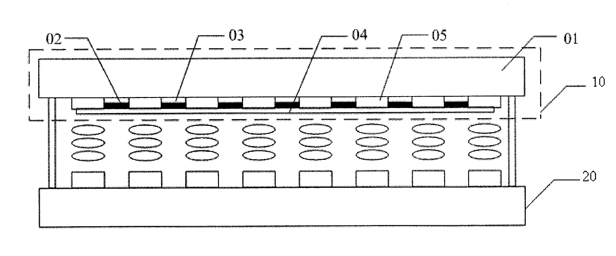
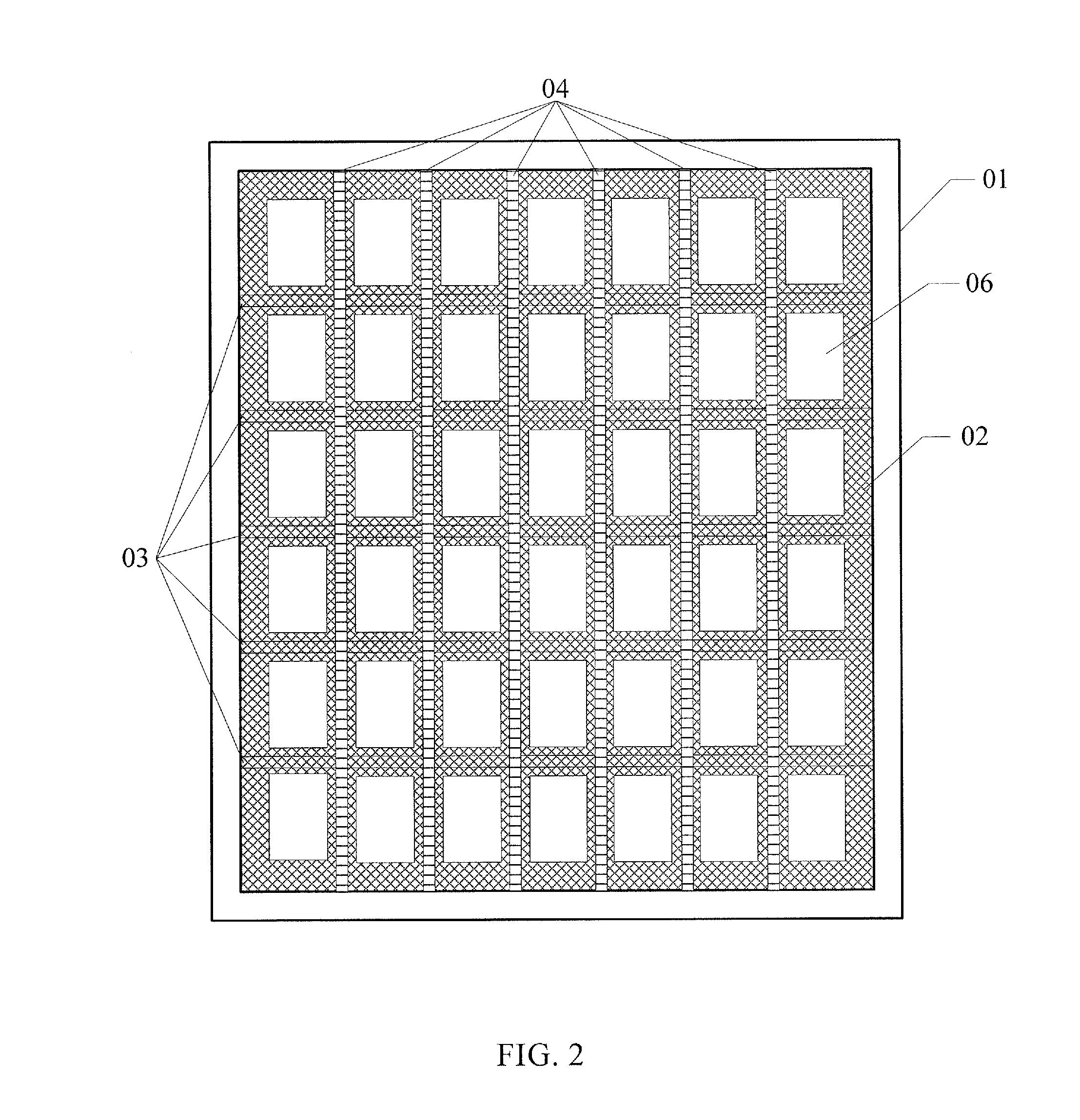
[0037]As shown in FIG. 1, ...


PUM


Abstract

The present disclosure relates to a capacitive in-cell touch screen panel and a display device in which first touch detecting electrodes and second touch detecting electrodes insulated with each other are provided on a substrate; the first touch detecting electrodes are located between the substrate and the black matrix, the second touch detecting electrodes are located on a side of the black matrix away from the substrate. Because the first touch detecting electrodes and the second touch detecting electrodes are provided on the substrate away from the TFT array substrate, it is possible to avoid mutual interference between touch signals and display signals in the TFT array substrate, thereby not only ensuring the quality of pictures on a liquid crystal display but also enhancing reliability of touch operations.

Description

TECHNICAL FIELD[0001]The present disclosure relates to a capacitive in-cell touch screen panel and a display device.BACKGROUND[0002]With the fast development of display technology, touch screen panels have gradually become popular in people's life. At present, based on the constituting structures, touch screen panels can be classified into add-on mode touch screen panels, on-cell touch screen panels, and in-cell touch screen panels. For add-on mode touch screen panels, the touch screen panel and the liquid crystal display are produced separately and then attached together to form a liquid crystal display with touch function, which suffer disadvantages such as high manufacturing costs, low light transmission ratio, and great thickness of modules. For in-cell touch screen panels, touch electrodes of the touch screen panel are embedded inside the liquid crystal display, which can reduce the overall thickness of the module and also greatly decrease manufacturing costs of touch screen pa...

Claims


Application Information

Patent Timeline
Patent Type & Authority Applications(United States)
IPC IPC(8): G06F3/044
CPCG06F3/044G06F3/0412G06F2203/04112G06F3/0445G06F3/0446G06F3/0448G06F3/0443
Inventor WANG, CHUNLEIDONG, XUECHE, CHUNCHENGXUE, HAILINWANG, HAISHENGWANG, LEIXIE, JIANYUNYANG, SHENGJIZHAO, WEIJIE
Owner BEIJING BOE OPTOELECTRONCIS TECH CO LTD
Why Eureka
Try Eureka