
Capacitive touch display panel, capacitive touch panel and manufacturing method thereof

a capacitive touch display and capacitive technology, applied in the field of capacitive touch display panel and capacitive touch panel, can solve the problems of lowering the user's willingness to use and influencing the user's visual experience, and achieve the effect of being seen by users

Active Publication Date: 2015-06-18
AU OPTRONICS CORP
View PDF13 Cites 17 Cited by
  • Summary
  • Abstract
  • Description
  • Claims
  • Application Information

AI Technical Summary

Benefits of technology

This patent describes an improved capacitive touch display panel that solves the problem of metal bridge lines being easily visible to the user. The panel has a low reflection pattern layer that is accurately placed on top of the opaque bridge lines, which reduces the amount of light reflected and maintains a high display aperture ratio, improving the user's visual experience. The invention is also a manufacturing method for this capacitive touch panel.

Problems solved by technology

However, since the metal has greater reflectivity, it is likely to reflect ambient light and generate bright spots or bright lines, and thus a user is very easy to see bright spots or bright lines at whereby the bridge lines are located, thereby influencing the user's visual experience and lowering the user's willingness to use.

Method used


Image

  • Capacitive touch display panel, capacitive touch panel and manufacturing method thereof
  • Capacitive touch display panel, capacitive touch panel and manufacturing method thereof
  • Capacitive touch display panel, capacitive touch panel and manufacturing method thereof

Examples


Embodiment Construction

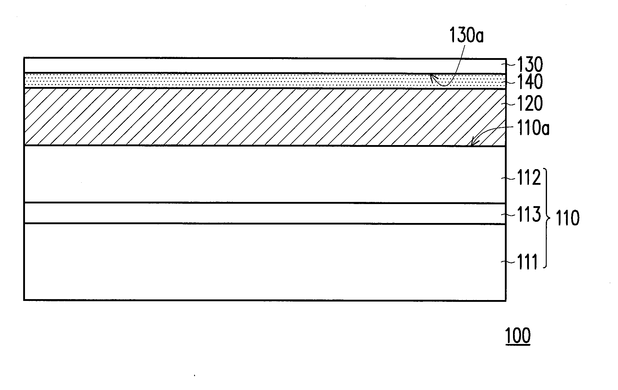
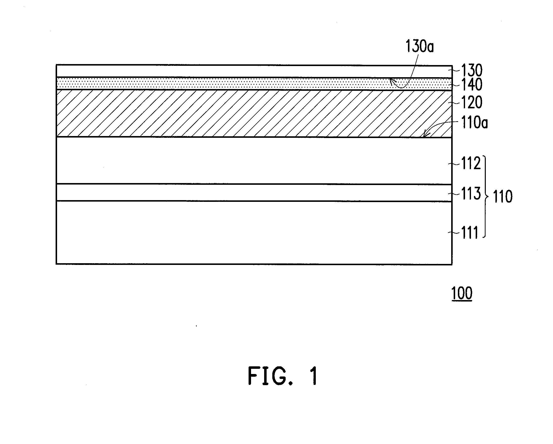
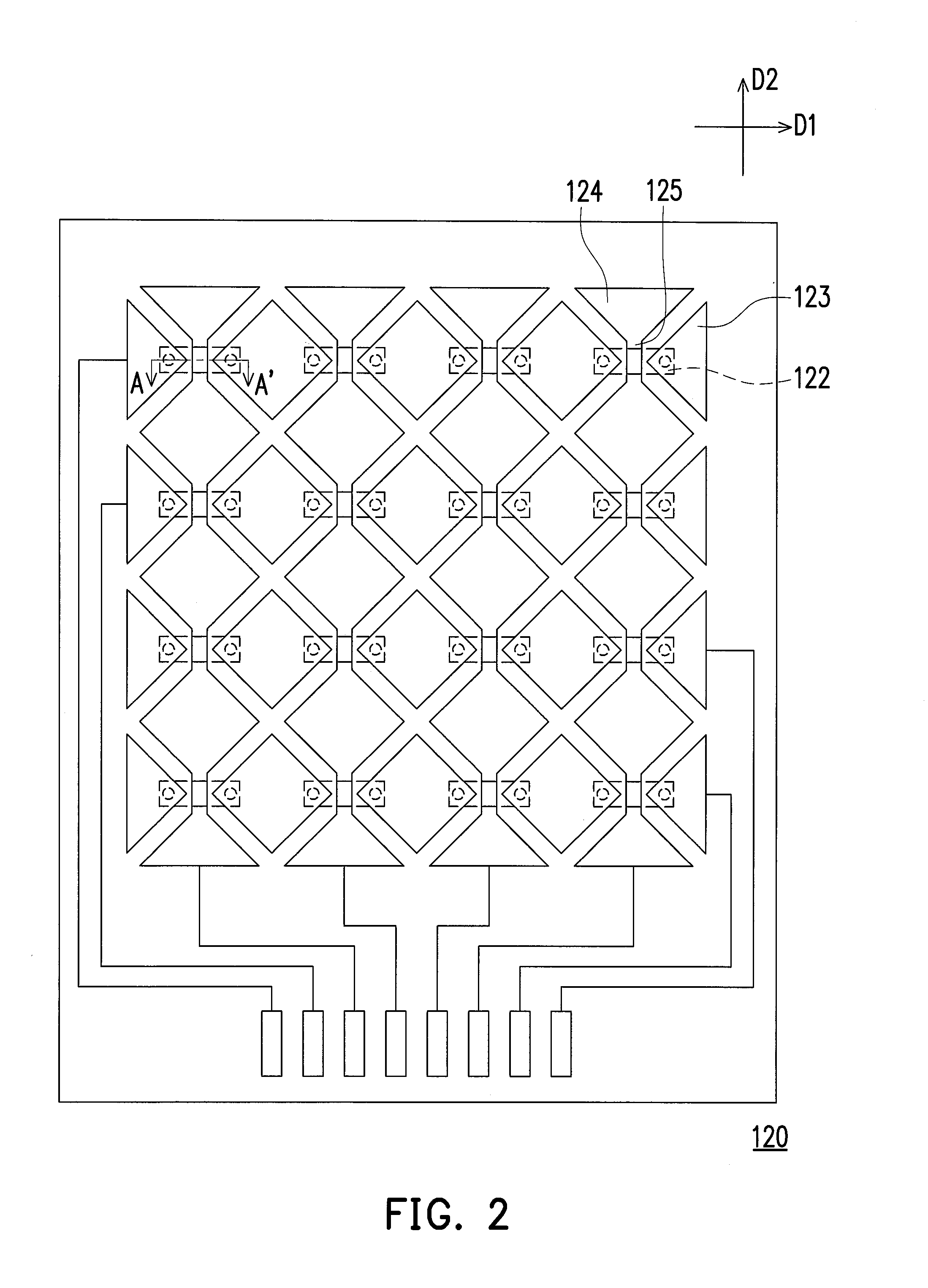
[0048]FIG. 1 is a schematic cross-sectional diagram illustrating a capacitive touch display panel according to an embodiment of the invention. Referring to FIG. 1, a capacitive touch display panel 100 includes a display panel 110 and a capacitive touch device 120. The display panel 110 has a display surface 110a, and the capacitive touch device 120 is disposed on the display surface 110a of the display panel 110. For instance, the display panel 110 of the present embodiment includes a pixel array substrate 111, a color filter substrate 112 and a display medium layer 113, wherein the display medium layer 113 is located between the pixel array substrate 111 and the color filter substrate 112. The capacitive touch device 120 is disposed at a side of the color filter substrate 112 that is relatively away from the display medium layer 113. In other words, the capacitive touch display panel 100 of the present embodiment is an on-cell capacitive touch display panel. It is to be explained t...


PUM


Abstract

A capacitive touch display panel including a display panel and a capacitive touch device is provided. The capacitive touch device is disposed on a display surface of the display panel. The capacitive touch device includes at least one opaque bridge line and at least one low reflection pattern layer. The opaque bridge line has a first linewidth and two first main borders. The low reflection pattern layer is disposed on a side of the opaque bridge that is opposite to the display panel. The low reflection pattern layer has a second linewidth and two second main borders. The low reflection pattern layer overlaps the opaque bridge line in a vertical projection direction. The first line width is substantially equal to the second line width, and the first main borders are substantial aligned to the second main borders. A capacitive touch panel and a manufacturing method thereof are provided, too.

Description

CROSS-REFERENCE TO RELATED APPLICATION[0001]This application claims the priority benefit of Taiwan application serial no. 102146714, filed on Dec. 17, 2013. The entirety of the above-mentioned patent application is hereby incorporated by reference herein and made a part of this specification.BACKGROUND[0002]1. Field of the Application[0003]The invention relates to a touch display panel, a touch panel and a manufacturing method thereof, and more particularly, to a capacitive touch display panel, a capacitive touch panel and a manufacturing method thereof.[0004]2. Description of Related Art[0005]Touch panels are roughly grouped into resistive touch panels, capacitive touch panels, optical touch panels, acoustic wave touch panels and electromagnetic touch panels according to different sensing methods thereof. The capacitive touch panels having advantages of fast response speed, favorable reliability, and durability have been extensively in electronic devices.[0006]In general, the capac...

Claims


Application Information

Patent Timeline
IPC IPC(8): G06F3/044
CPCG06F2203/04103G06F3/044G06F2203/04111G06F3/0443G06F3/0446
Inventor TUNG, TENG-FU
Owner AU OPTRONICS CORP
Learn More