Identifying layout pattern candidates

a technology of layout pattern and layout pattern, which is applied in the field of identifying layout pattern candidates, can solve the problems of increasing the complexity of the manufacturing process of these devices, the complexity of the design of the most complicated device ever engineered by man, and the complexity of the process of manufacturing these devices

Active Publication Date: 2015-08-13
SYNOPSYS INC
View PDF2 Cites 11 Cited by
  • Summary
  • Abstract
  • Description
  • Claims
  • Application Information

AI Technical Summary

Problems solved by technology

Some of the most complicated devices ever engineered by man are semiconductor integrated circuits.
Some circuits such as microprocessors may include a billion transistors or more, and are getting more complicated in their design every year.
In addition, the process of manufacturing these devices is getting

Method used


Image

  • Identifying layout pattern candidates
  • Identifying layout pattern candidates
  • Identifying layout pattern candidates

Examples


Embodiment Construction

[0018]Processes and devices may be implemented and utilized for automatically identifying layout pattern candidates in selected regions for use in analyzing performance issues. These processes and apparatuses may be implemented and utilized as will be explained with reference to the various embodiments below.

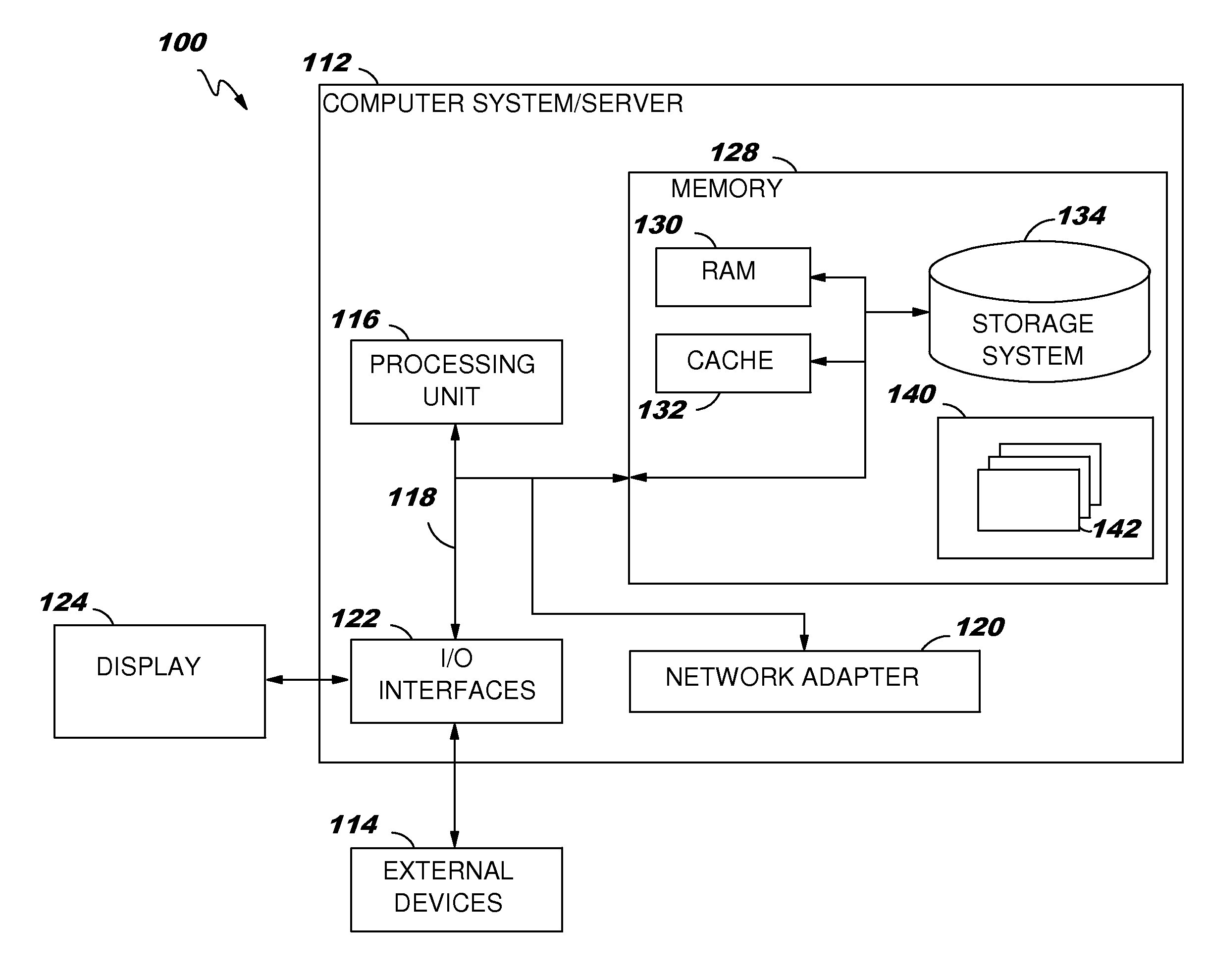
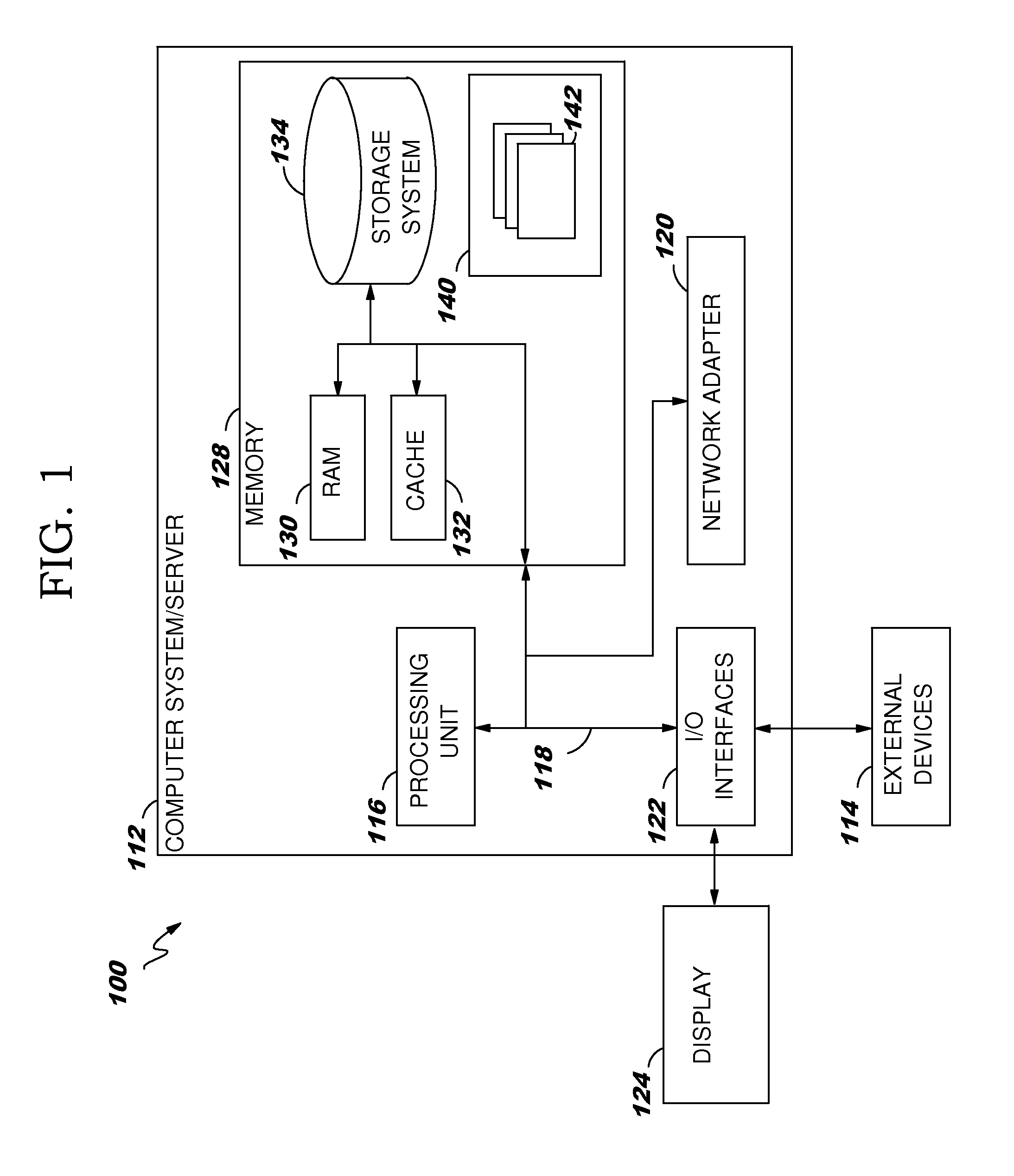
[0019]FIG. 1 is a block diagram of an illustrative data processing system in which various embodiments of the present disclosure may be implemented. Data processing system 100 is one example of a suitable data processing system and is not intended to suggest any limitation as to the scope of use or functionality of the embodiments described herein. Regardless, data processing system 100 is capable of being implemented and / or performing any of the functionality set forth herein such as automatically identifying layout pattern candidates in selected regions for use in analyzing performance issues.

[0020]In data processing system 100 there is a computer system / server 112, which is o...


PUM


Abstract

A method, system or computer usable program product for automatically identifying layout pattern candidates in selected regions for use in analyzing semiconductor device performance issues including identifying a set of target regions and a set of reference regions from a design layout; utilizing a processor to generate a reference baseline of layout patterns from the set of reference regions; utilizing the processor to compare a frequency profile of layout patterns in the set of target regions to a frequency profile of layout patterns in the reference baseline; and based on the comparison, utilizing the processor to identify candidate layout patterns from the set of target regions for further analysis.

Description

BACKGROUND[0001]1. Technical Field[0002]The present invention relates generally to identifying layout pattern candidates, and in particular, to a computer implemented method for automatically identifying layout pattern candidates in selected regions for use in analyzing performance issues.[0003]2. Description of Related Art[0004]Some of the most complicated devices ever engineered by man are semiconductor integrated circuits. Some circuits such as microprocessors may include a billion transistors or more, and are getting more complicated in their design every year. In addition, the process of manufacturing these devices is getting more difficult and complicated as semiconductor manufacturing processes continue to develop the ability to manufacture smaller elements and more dense integrated circuits. This includes the use of photomasks that are denser and more complicated for patterning these smaller elements on semiconductor wafers.[0005]As a result, testing throughout the design an...

Claims


Application Information

Patent Timeline
IPC IPC(8): G06F17/50
CPCG06F17/5081G06F2217/68G06F2217/06G06F30/398G06F2111/04G06F2115/10
Inventor GORDON, BRIAN S.MARUTYAN, RAFIKKIM, JOHNSUZOR, CHRISTOPHE P.
Owner SYNOPSYS INC
Why Eureka
Try Eureka