Individually read-accessible twin memory cells

Active Publication Date: 2015-12-03
STMICROELECTRONICS (ROUSSET) SAS
View PDF3 Cites 15 Cited by
  • Summary
  • Abstract
  • Description
  • Claims
  • Application Information

AI Technical Summary

Benefits of technology

[0013]It can thus also be desired to provide another improvement of this memory array and memory cell stru

Problems solved by technology

This causes a noticeable complexification of the word line and column decoders, and includes providing

Method used


Image

  • Individually read-accessible twin memory cells
  • Individually read-accessible twin memory cells
  • Individually read-accessible twin memory cells

Examples


Embodiment Construction

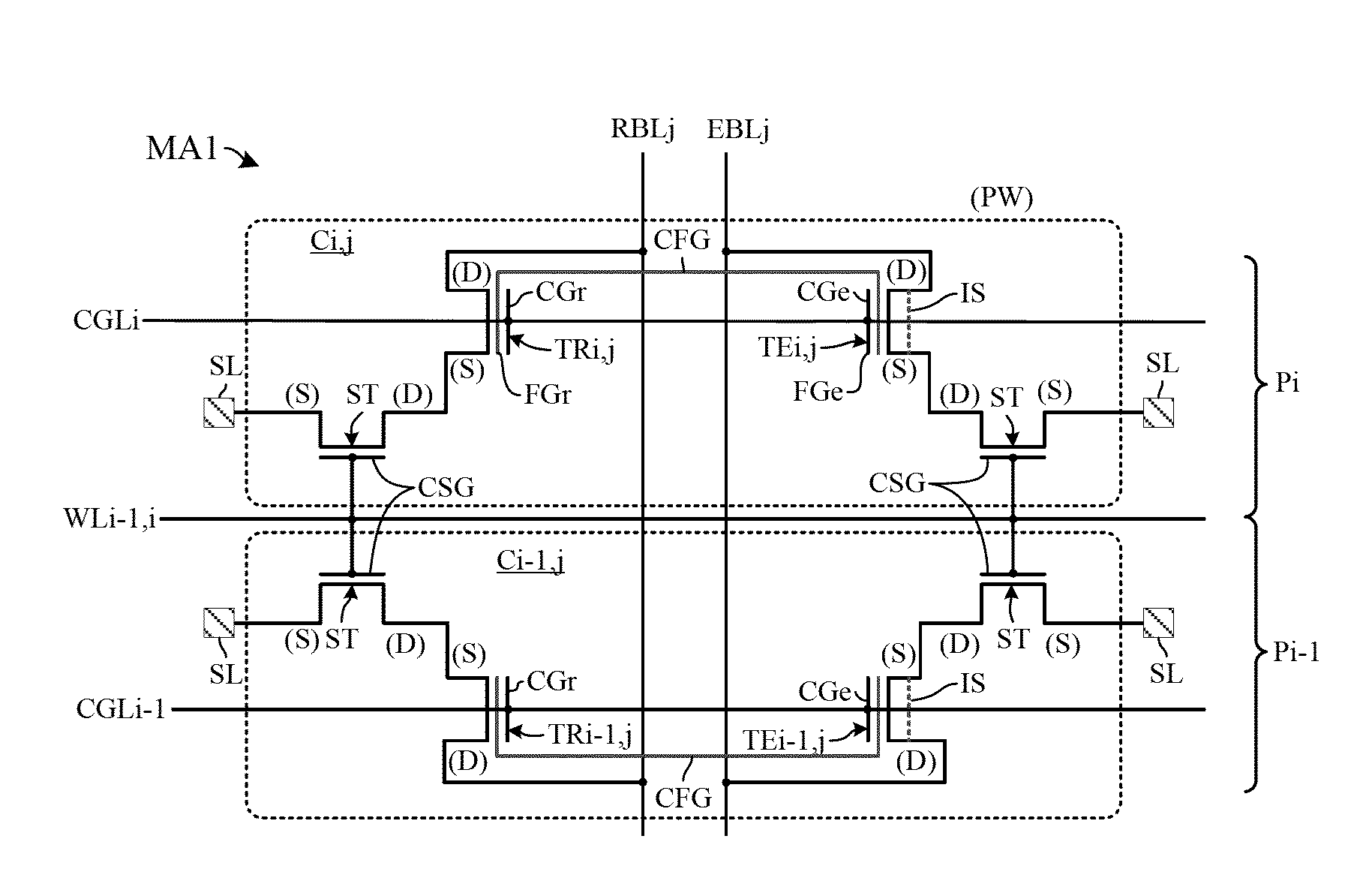
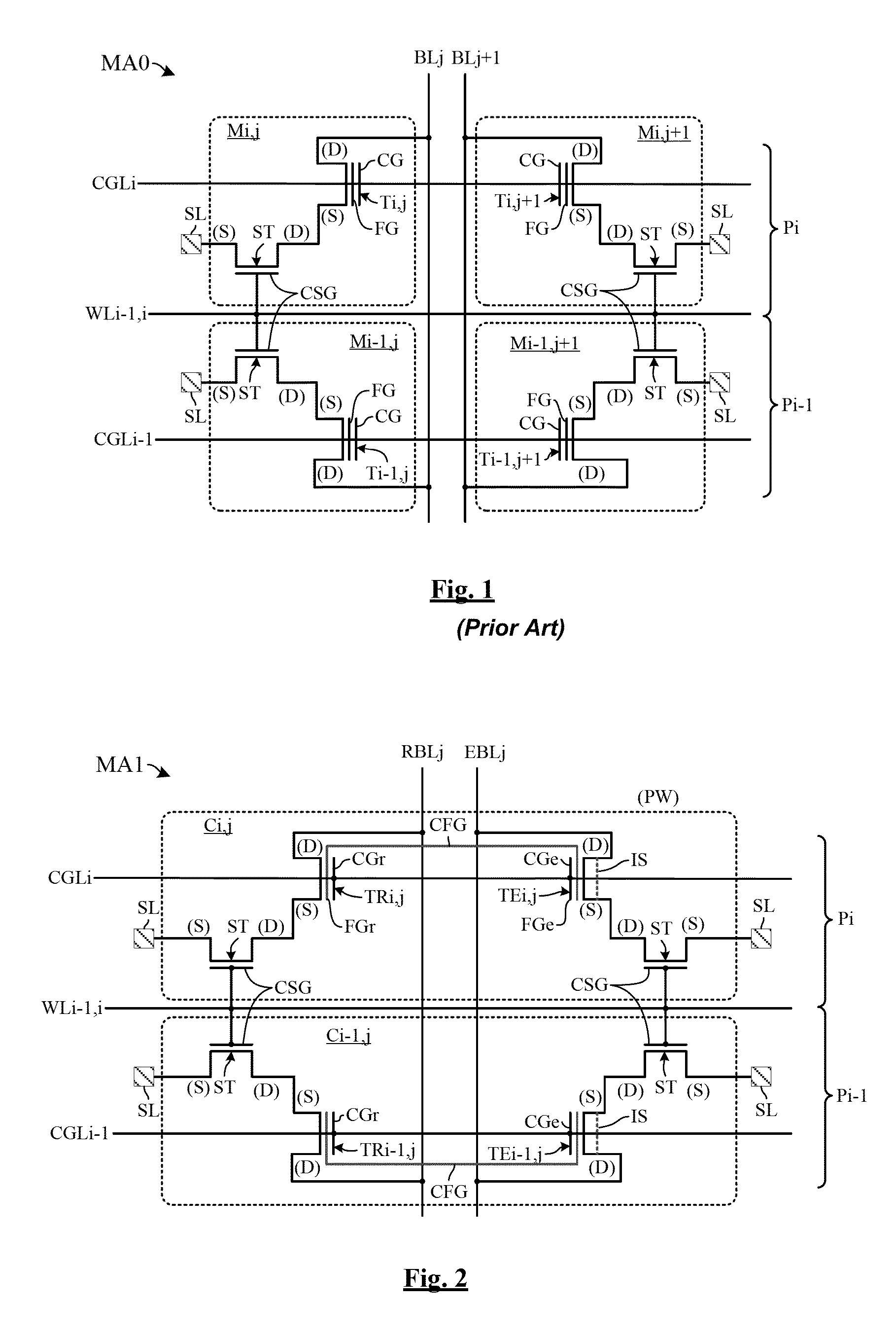
[0050]FIG. 2 is the wiring diagram of one embodiment of two memory cells Ci,j, Ci−1,j and of a memory array MA1 according to a first improvement according to the present disclosure of the memory array and memory cell structure in FIG. 1.

[0051]The memory cells are read- and write-accessible via a first bit line RBLj, a second bit line EBLj, a word line WLi−1,i, and two control gate lines CGLi, CGLi−1. The memory cell Ci,j belongs to a physical page Pi of the memory array and the memory cell Ci−1,j belongs to an adjacent page Pi−1. The pages Pi, Pi−1 may comprise various other memory cells and the memory array MA1 may comprise various other pages.

[0052]The memory cell Ci,j comprises two floating-gate transistors TRi,j, TEi,j the floating gates FGr, FGe of which are interconnected, the floating-gate transistor TRi,j being dedicated to reading the transistor memory cell and the floating-gate transistor TEi,j being dedicated to erasing the memory cell. According to one embodiment, the fl...


PUM


Abstract

The present disclosure relates to a non-volatile memory on a semiconductor substrate, comprising: a first memory cell comprising a floating-gate transistor and a select transistor having an embedded vertical control gate, a second memory cell comprising a floating-gate transistor and a select transistor having the same control gate as the select transistor of the first memory cell, a first bit line coupled to the floating-gate transistor of the first memory cell, and a second bit line coupled to the floating-gate transistor of the second memory cell.

Description

BACKGROUND[0001]1. Technical Field[0002]The present disclosure relates to non-volatile memories and in particular to a memory array and memory cell structure of the type described in the US application 2013 / 0228846.[0003]2. Description of the Related Art[0004]As a reminder, FIG. 1 represents such a memory array structure MA0 and shows memory cells Mi,j, Mi−1,j, Mi,j+1, Mi−1,j+1 of the above-mentioned type, belonging here to two adjacent physical pages Pi, Pi−1 of the memory array, of respective ranks “i” and “i−1”. The memory cells Mi,j, Mi−1, Mi,j+1, Mi−1,j+1 are read- and write-accessible through bit lines BLj, BLj+1, a word line WLi−1,i and control gate lines CGLi, CGLi−1. Each memory cell comprises a floating-gate transistor, respectively Ti,j, Ti−1, Ti,j+1, Ti−1,j+1. The drain terminals D of the transistors Ti,j, Ti−1,j are connected to the bit line BLj and the drain terminals of the transistors Ti,j+1, Ti−1,j+1 are connected to the bit line BLj+1. The control gates CG of the t...

Claims


Application Information

Patent Timeline
IPC IPC(8): H01L27/115G11C16/26H01L29/788H01L21/28H01L29/06H01L23/528H01L29/423G11C16/14H01L29/66
CPCH01L27/11524G11C16/14G11C16/26H01L29/7889H01L21/28008H01L29/0649H01L27/11519H01L23/528H01L29/42328H01L29/66825G11C16/0433G11C16/0441H01L29/7883H01L2924/0002H10B41/35H01L2924/00H10B41/10
Inventor LA ROSA, FRANCESCONIEL, STEPHANREGNIER, ARNAUD
Owner STMICROELECTRONICS (ROUSSET) SAS
Why Eureka
Try Eureka