Method and apparatus for selective deposition

Active Publication Date: 2016-01-07
APPLIED MATERIALS INC
View PDF2 Cites 160 Cited by
  • Summary
  • Abstract
  • Description
  • Claims
  • Application Information

AI Technical Summary

Problems solved by technology

However, in cases when a substrate only contains one type of material, the self assembled monolayer (SAM) 210 may be globa

Method used


Image

  • Method and apparatus for selective deposition
  • Method and apparatus for selective deposition
  • Method and apparatus for selective deposition

Examples


Embodiment Construction

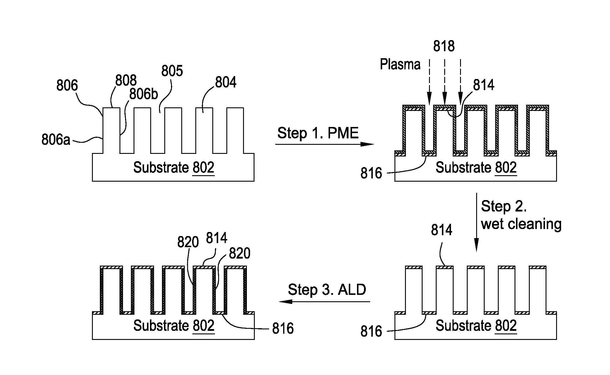
[0027]Methods for selectively depositing different materials at different locations on a structure formed on the substrate are provided. The structure may include a fin structure, a gate structure, a contact structure, or any suitable structure in semiconductor devices, particularly for three dimensional (3D) stacking of fin field effect transistor (FinFET) semiconductor structures. In one embodiment, a selective deposition process may form different materials on different surfaces, e.g., different portions of a structure, wherein the structure is comprised of a single material. For example, the described methods may use ion assisted directional plasma treatment (PME) to sequentially or simultaneously treat different regions of a 3D structure by utilizing ion implantation at one or more selected angles into the designated regions of the substrate having the 3D structure formed thereon. The ions modify surface properties of a portion of the substrate or the first deposition material,...


PUM

PropertyMeasurementUnit
Angleaaaaaaaaaa
Angleaaaaaaaaaa
Angleaaaaaaaaaa

Abstract

Methods for forming fin structures with desired materials formed on different locations of the fin structure using a selective deposition process for fin field effect transistors (FinFETs) are provided. In one embodiment, a method of forming a structure with desired materials on a substrate includes depositing a first material on a substrate having a three-dimensional (3D) structure formed thereon while performing an implantation process to dope a first region of the 3D structure. The first material may be removed and a second material may be deposited on the 3D structure. The second material may selectively grow on a second region of the 3D structure.

Description

CROSS-REFERENCE TO RELATED APPLICATIONS[0001]This application claims benefit of U.S. Provisional Patent Application No. 62 / 020,651, filed Jul. 3, 2014, the entirety of which is herein incorporated by reference.BACKGROUND[0002]1. Field[0003]Embodiments described herein generally relate to methods for forming three dimensional structures, such as fin field effect transistors (FinFETs) on a semiconductor substrate. More specifically, embodiments relate to methods for forming three dimensional structures on a semiconductor substrate with different materials at different locations of the structure by utilizing a selective deposition process.[0004]2. Description of the Related Art[0005]FIG. 1A (Prior Art) depicts an exemplary embodiment of a fin field effect transistor (FinFET) 150 disposed on a substrate 100. The substrate 100 may be a silicon substrate, a germanium substrate, or a substrate formed from other semiconductor materials. In one embodiment, the substrate 100 may include p-typ...

Claims


Application Information

Patent Timeline
IPC IPC(8): H01L29/66H01L21/02H01L21/223H01L21/265H01L21/266
CPCH01L29/66803H01L21/26513H01L21/0262H01L21/266H01L21/02057H01L21/2236C23C16/0227C23C16/04C23C16/455C23C16/45525H01L21/0228H01J37/32403H01J37/32422H01J37/32623H01L21/205H01L21/02315H01L21/02296H01L21/02334C23C16/45536
Inventor YIEH, ELLIE Y.NEMANI, SRINIVAS D.GODET, LUDOVICFAN, YINMA, TRISTAN
Owner APPLIED MATERIALS INC
Why Eureka
Try Eureka