Testable power-on-reset circuit

a power-on-reset and circuit technology, applied in the field of integrated circuits, can solve the problems of affecting the performance of the ic, or destroying the ic or setting the ic in an indeterminate state,

Active Publication Date: 2016-02-25
NXP USA INC
View PDF9 Cites 6 Cited by
  • Summary
  • Abstract
  • Description
  • Claims
  • Application Information

AI Technical Summary

Problems solved by technology

However, during ramp-up, the supply voltage level is less than the operating voltage level for a short time, at which time the digital and analog components of the IC may malfunction and possibly damage the IC or set the IC in an indeterminate state.
If the POR de-assertion threshold exceeds the optimum voltage level, the IC remains in the reset mode, which delays the IC from being ready to function after power-up.
Thus, the performance of the IC is negatively impacted.
If the POR de-assertion threshold is less than the optimum voltage level, the digital and analog components may not be properly reset and thus may cause functional errors.
This method of testing the POR circuit requires the addition of a dedicated analog test pad, which is undesirable due to the increased cost of adding the analog test pad.
However, the supply voltage required for the processor core to operate and poll the output of the test flip-flop exceeds the optimum voltage level of the POR circuit, so by the time the processor core can monitor the flip-flop, the POR de-assertion threshold has already been exceeded, so this method is not accurate.
However, this method requires the first set of IO pads and the driver circuit, which increase the area overhead and power consumption of the IC.

Method used


Image

  • Testable power-on-reset circuit
  • Testable power-on-reset circuit
  • Testable power-on-reset circuit

Examples


Embodiment Construction

[0015]The detailed description of the appended drawings is intended as a description of the currently preferred embodiments of the present invention, and is not intended to represent the only form in which the present invention may be practiced. It is to be understood that the same or equivalent functions may be accomplished by different embodiments that are intended to be encompassed within the spirit and scope of the present invention.

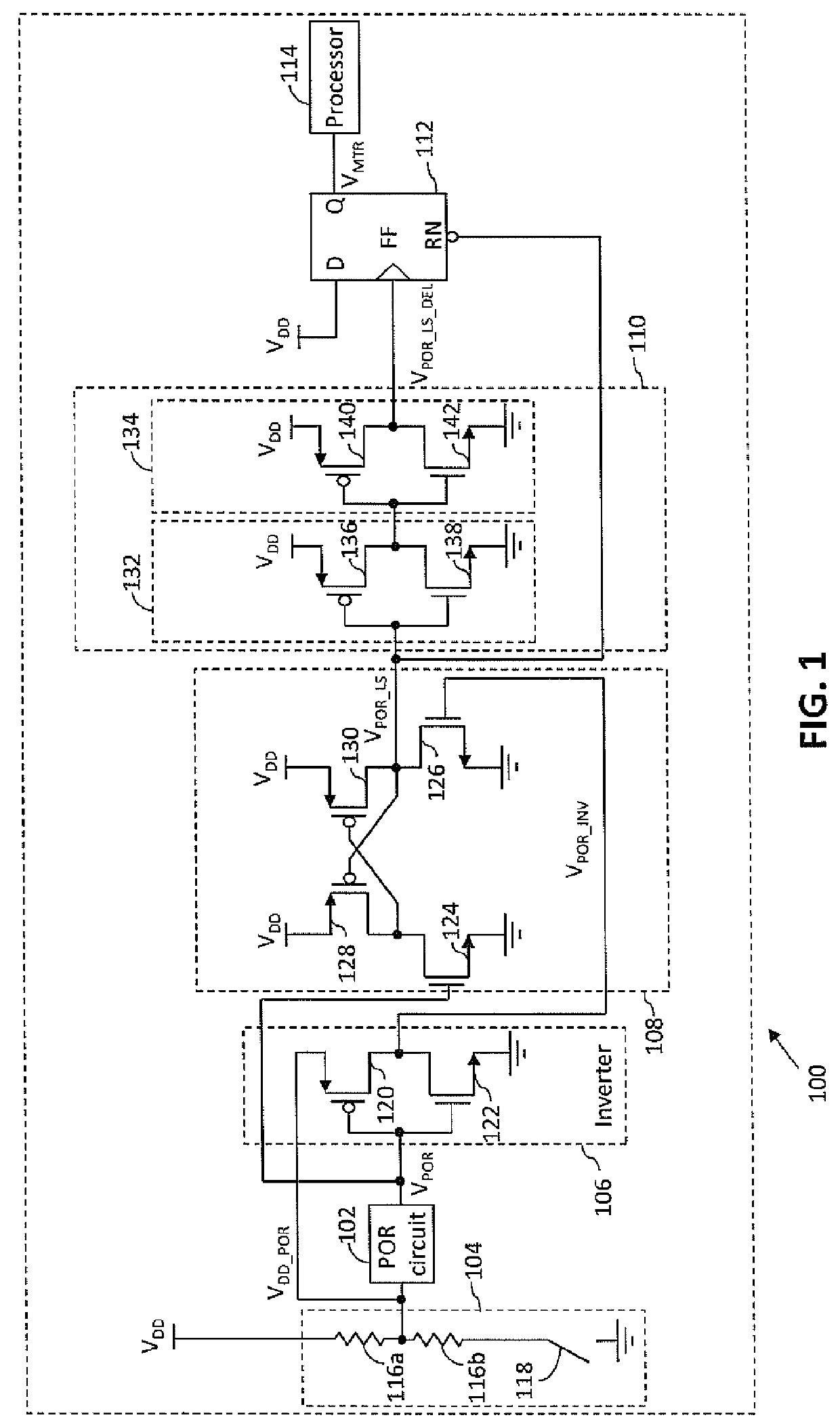
[0016]In an embodiment of the present invention, an integrated circuit with a testable power-on-reset (POR) circuit is provided. The integrated circuit includes a voltage divider, the POR circuit, an inverter, a level-shifter, a buffer, and a flip-flop. The voltage divider receives a first supply voltage and outputs a second supply voltage. The POR circuit is connected to the voltage divider for receiving the second supply voltage and generating a POR voltage signal when the second supply voltage exceeds a POR de-assertion threshold. The inverter is ...


PUM


Abstract

An integrated circuit with a testable power-on-reset (POR) circuit includes a voltage divider, an inverter, a level-shifter, a buffer and a flip-flop. The voltage divider receives a first supply voltage and generates a second supply voltage. The POR circuit receives the second supply voltage and generates a POR voltage signal when the second supply voltage exceeds a POR de-assertion threshold. The level-shifter receives the POR voltage signal and an inverted POR voltage signal from the inverter circuit and generates a level-shifted POR voltage signal at a voltage level of the first supply voltage. The buffer receives the level-shifted POR voltage signal and outputs a delayed level-shifted POR voltage signal. The flip-flop receives the first supply voltage as data input, the delayed level-shifted POR voltage signal as clock input, the level-shifted POR voltage signal as reset input, and outputs a voltage-monitor signal at the voltage level of the first supply voltage.

Description

BACKGROUND OF THE INVENTION[0001]The present invention generally relates to integrated circuits, and, more particularly, to power-on-reset circuits.[0002]Many integrated circuits (ICs) including system-on-chip (SoC) integrate various digital and analog components on a single chip. The components may include sequential elements such as flip-flops and combinational elements such as multiplexers and encoders. Such ICs are connected to external voltage sources for receiving supply voltages and the digital and analog components operate at a supply voltage level generated by the external voltage source. The IC is powered down by switching off the external voltage source, and when powered back on, the device is reset.[0003]The IC is powered on by switching on the external voltage source. The supply voltage level received by the IC gradually ramps-up to the operating voltage level. However, during ramp-up, the supply voltage level is less than the operating voltage level for a short time, a...

Claims


Application Information

Patent Timeline
Patent Type & Authority Applications(United States)
IPC IPC(8): H03K17/22H03K19/0185
CPCH03K17/223H03K3/0375H03K17/22H03K19/018521
Inventor WADHWA, SANJAY KUMARTRIPATHI, AVINASH CHANDRA
Owner NXP USA INC
Why Eureka
Try Eureka