Power detecting circuit and method for stable power-on reading of flash memory device using the same

a power detection circuit and flash memory technology, applied in electronic switching, digital storage, instruments, etc., can solve problems such as the abnormal read operation, the low-voltage memory device may be damaged, and the noise may be caused, so as to achieve the effect of stable power-on reading method

Inactive Publication Date: 2005-04-19
SAMSUNG ELECTRONICS CO LTD
View PDF5 Cites 35 Cited by
  • Summary
  • Abstract
  • Description
  • Claims
  • Application Information

AI Technical Summary

Benefits of technology

[0011]Embodiments of the invention also provide a stable power-on reading method for a memory device.

Problems solved by technology

However, noise may be caused by an unstable state of an external power supply voltage or excessive power consumption in the chip.
Since low-voltage memory devices are very sensitive to noise, problems such as this abnormal read operation may become more serious.

Method used


Image

  • Power detecting circuit and method for stable power-on reading of flash memory device using the same
  • Power detecting circuit and method for stable power-on reading of flash memory device using the same
  • Power detecting circuit and method for stable power-on reading of flash memory device using the same

Examples


Embodiment Construction

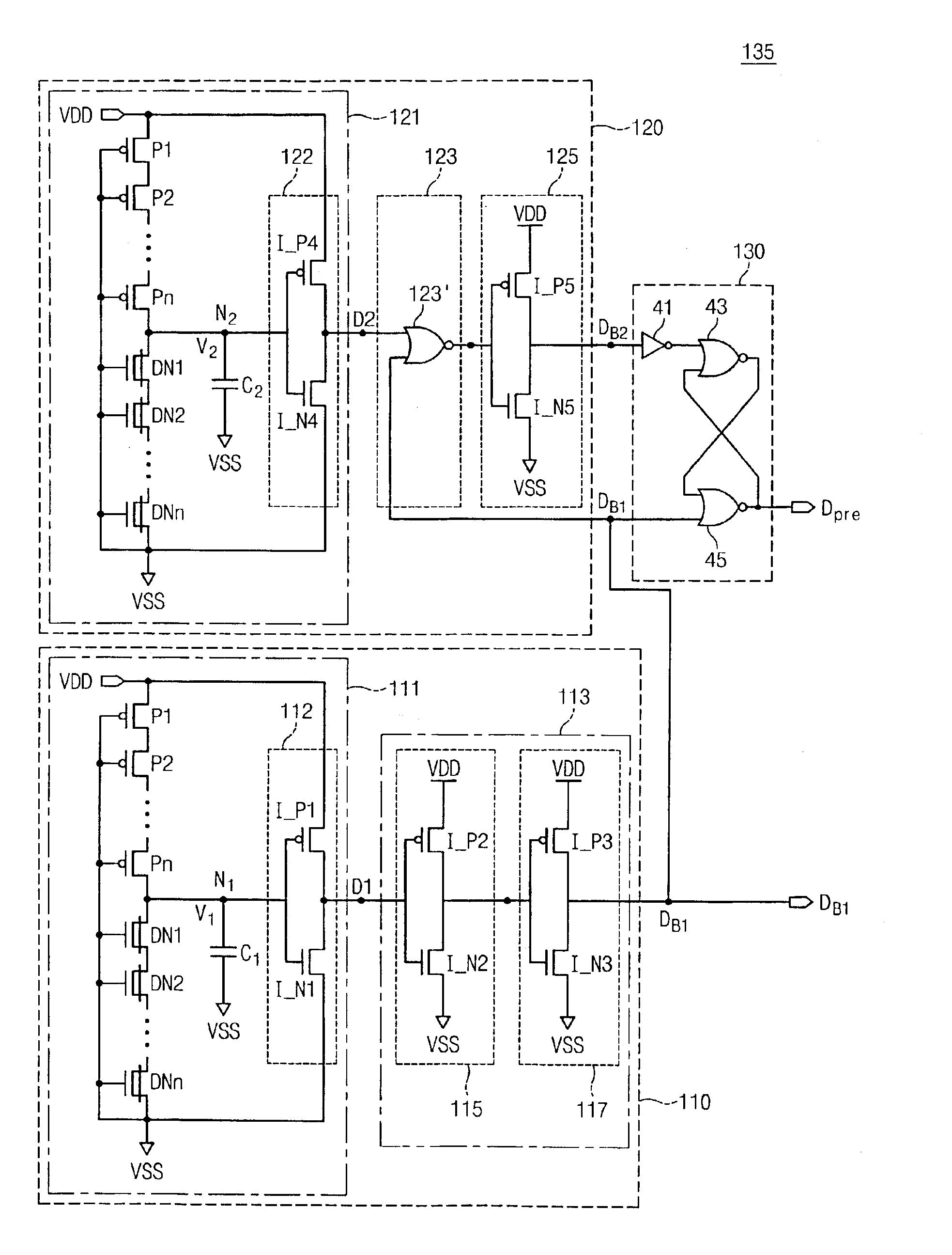
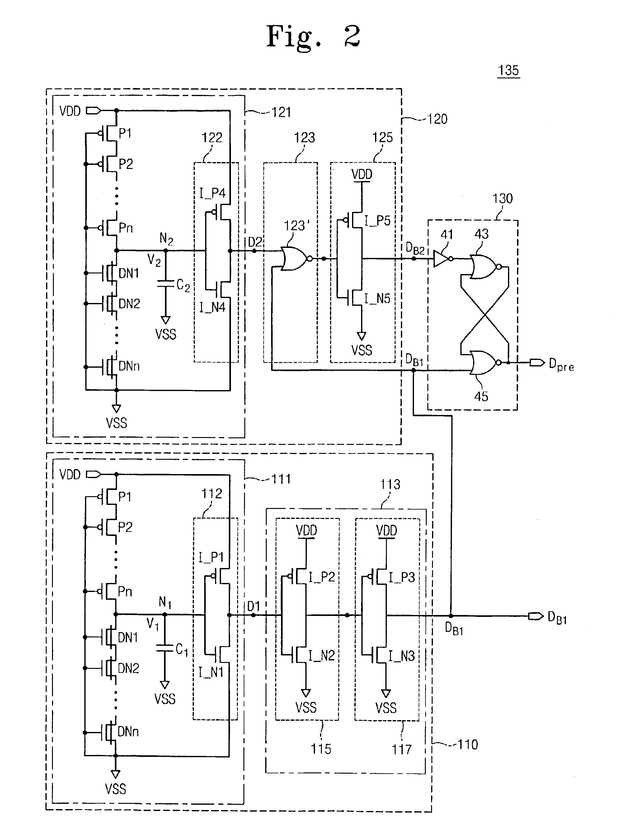
[0017]Embodiments of the invention will be more fully described with reference to the attached drawings of FIGS. 1 to 4. In the attached drawings, similar constituent elements are marked by the same or similar reference numerals or symbols, respectively.

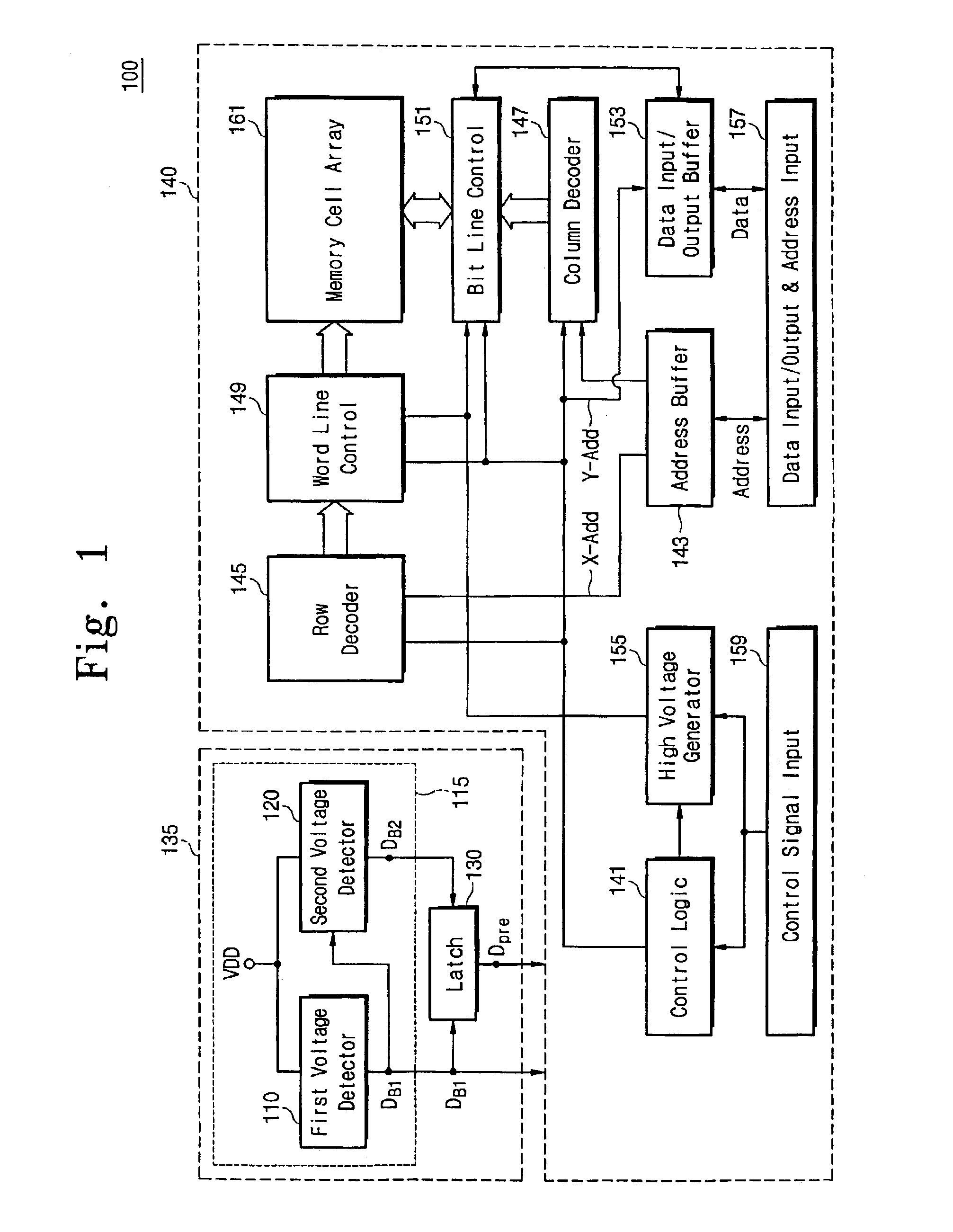
[0018]FIG. 1 schematically shows a flash memory device 100 according to an embodiment of the invention. A flash memory device 100 includes a power detecting circuit 135 and a memory chip 140.

[0019]The flash memory device 100 in FIG. 1 can be used in any system as a boot-up memory for storing boot-up information and as a general memory for storing information except for boot-up information. In a case where the flash memory device 100 is used as the boot-up memory, if logic circuits in the memory are initialized by the power detecting circuit 135 and a power-on read signal Dpre is enabled, an operation of reading out data (e.g., boot-up information) from a memory cell array 161 commences with reference to a previously designed algorith...


PUM


Abstract

Embodiments of the invention provide a power-on reset function that establishes logic circuits in a memory chip at an initial stable state and a power-on read function that triggers a read operation of the memory chip. A first voltage detector output signal transitions when a power supply voltage reaches a first voltage, setting the logic circuits at the initial stable state. A second voltage detector output signal transitions when the power supply voltage reaches a second voltage, placing a latch in a set state that results in activation of a power-on read signal. A power-on read operation is carried out according to the activation of the power-on read signal. If the power supply voltage is not lowered below the first voltage, the second voltage detector output signal does not transition. Accordingly, embodiments are capable of preventing power-on read operations that are unnecessarily performed owing to power noise.

Description

CROSS REFERENCE TO RELATED APPLICATIONS[0001]This application claims priority from Korean Patent Application No. 2002-29493, filed on May 28, 2002, the contents of which are herein incorporated by reference in their entirety for all purposes.BACKGROUND OF THE INVENTION[0002]1. Technical Field of the Invention[0003]This disclosure relates to a power detecting circuit of a semiconductor memory device, and in particular to a power detecting circuit having a power-on reset function and a power-on read function of a semiconductor memory device. Further disclosed is a method for generating a power-on reset signal and a power-on read signal.[0004]2. Description of the Related Art[0005]A semiconductor memory device includes an array of memory cells and a number of logic circuits for controlling the array. For example, the logic circuits may be formed of a number of latches and flip-flops. Logic circuits, and in particular, flip-flops and latches, must initially have states that are well-def...

Claims


Application Information

Patent Timeline
Patent Type & Authority Patents(United States)
IPC IPC(8): G11C16/22G11C16/30G11C16/06G11C5/14G06F1/26G11C7/00G11C16/02H03K17/16H03K17/22
CPCG11C5/147G11C16/30G11C16/225G11C7/00
Inventor BYEON, DAE-SEOKLEE, KYEONG-HAN
Owner SAMSUNG ELECTRONICS CO LTD
Why Eureka
Try Eureka