

Semiconductor device
- Summary
- Abstract
- Description
- Claims
- Application Information
AI Technical Summary
Benefits of technology
Problems solved by technology
Method used
Image

Examples
Embodiment Construction
[0029]Exemplary embodiments will be described below in more detail with reference to the accompanying drawings. The present invention may, however, be embodied in different forms and should not be construed as limited to the embodiments set forth herein. Rather, these embodiments are provided so that this disclosure will be thorough and complete, and will fully convey the scope of the present invention to those skilled in the art. Wherever possible, the same reference numbers will be used throughout the drawings to refer to the same or like parts. A detailed description of well known configurations or functions will be omitted when it may make the subject matter less clear.
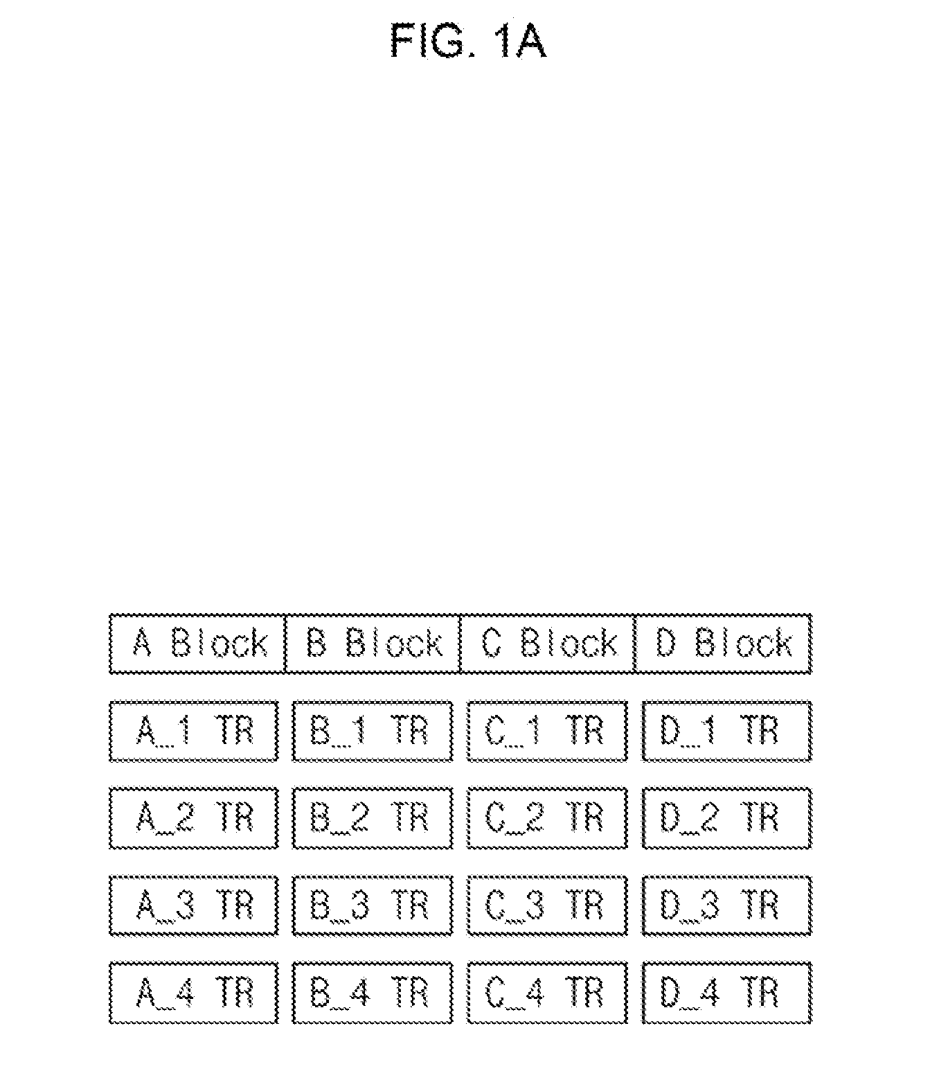
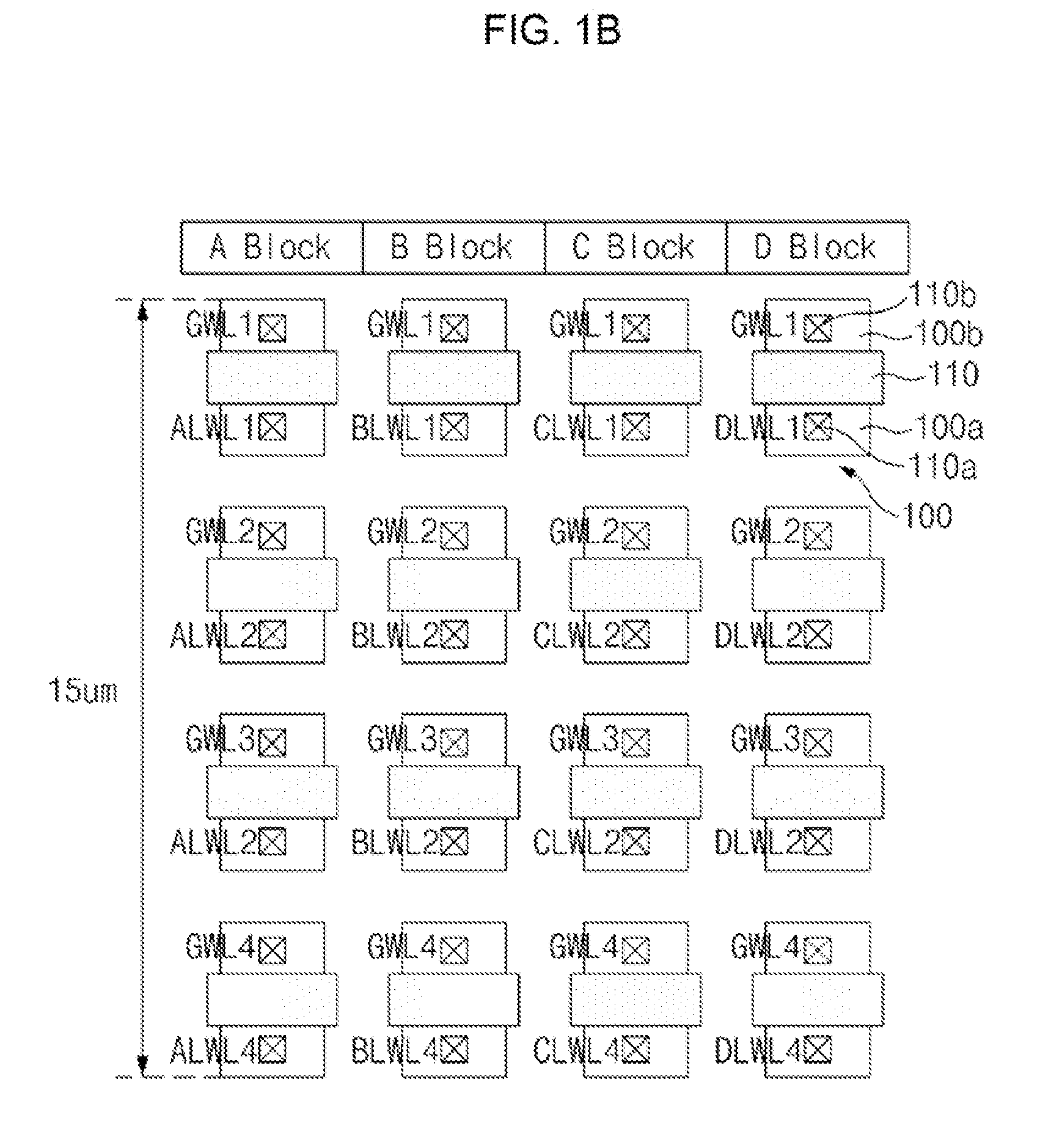
[0030]FIGS. 1A and 1B are schematic diagrams illustrating a pass transistor region of a conventional semiconductor device.
[0031]Referring to FIGS. 1A and 1B, a plurality of transistors, isolated from each other, may be arranged in one memory block, and each isolated transistor may be composed of one gate electrode...
PUM
 Abstract
Description
Claims
Application Information