

Light-emitting element, light-emitting device, electronic device, and lighting device
a technology of light-emitting elements and electronic devices, which is applied in the direction of electrical devices, semiconductor devices, organic semiconductor devices, etc., can solve the problems of difficult to inject holes into the el layer, difficult to achieve, and difficult to inject holes from the hole-transport layer to the host material of the light-emitting layer, etc., to achieve high emission efficiency and long life
- Summary
- Abstract
- Description
- Claims
- Application Information
AI Technical Summary
Benefits of technology
Problems solved by technology
Method used
Image

Examples
embodiment 1
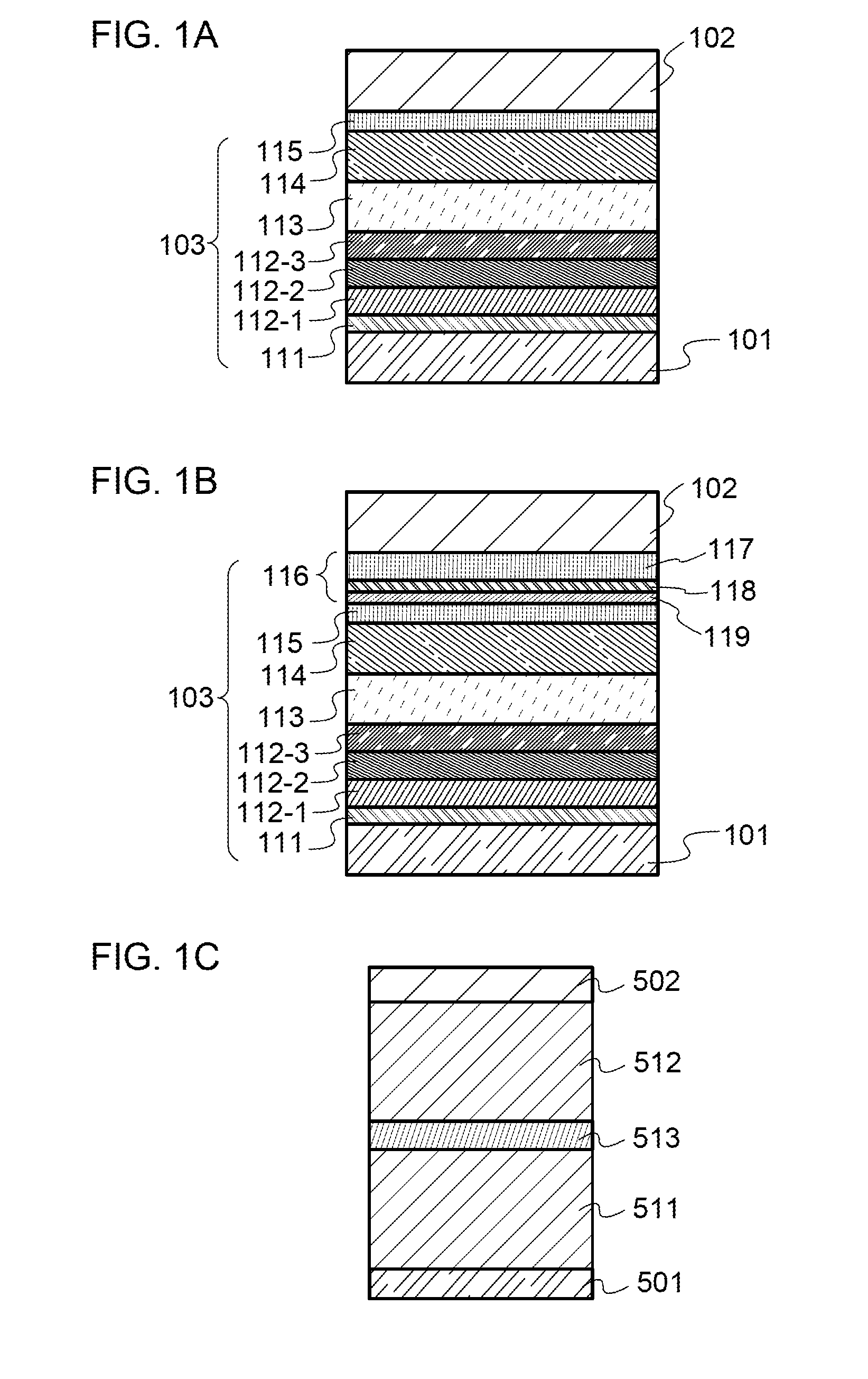
[0111]FIG. 1A illustrates a light-emitting element of one embodiment of the present invention. The light-emitting element of one embodiment of the present invention includes a first electrode 101, a second electrode 102, and an EL layer 103. The EL layer 103 includes a hole-injection layer 111, a first hole-transport layer 112-1, a second hole-transport layer 112-2, a third hole-transport layer 112-3, and a light-emitting layer 113 which are provided in this order from the first electrode 101 side. Furthermore, the EL layer 103 may further include an electron-transport layer 114 and an electron-injection layer 115.
[0112]In the light-emitting element of one embodiment of the present invention, the light-emitting layer 113 includes a host material and a light-emitting material; the hole-injection layer 111 includes an organic acceptor; and the first hole-transport layer 112-1, the second hole-transport layer 112-2, and the third hole-transport layer 112-3 include a first hole-transpor...
embodiment 2
[0168]In this embodiment, a light-emitting device including the light-emitting element described in Embodiment 1 is described.
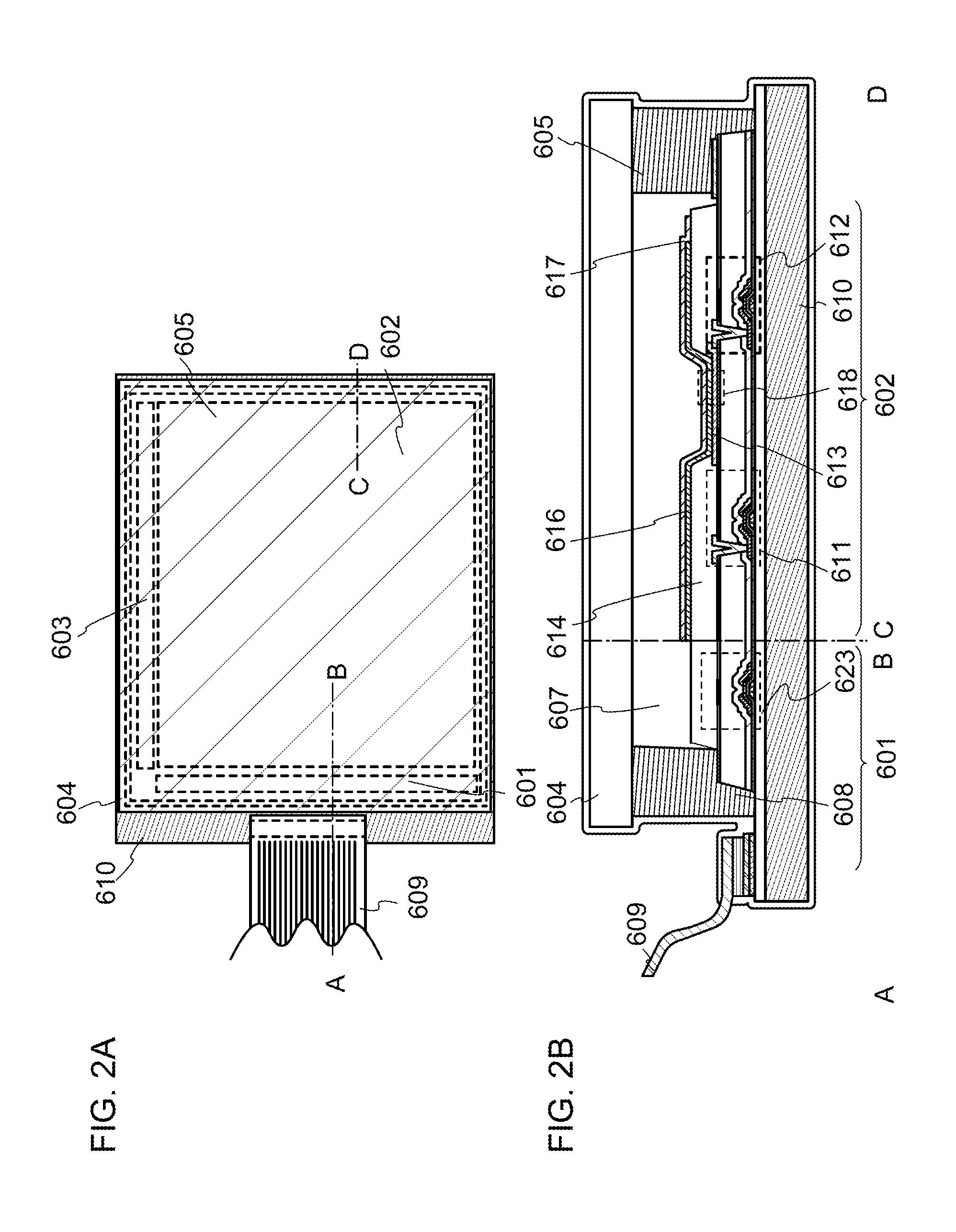
[0169]In this embodiment, the light-emitting device manufactured using the light-emitting element described in Embodiment 1 is described with reference to FIGS. 2A and 2B. Note that FIG. 2A is a top view of the light-emitting device and FIG. 2B is a cross-sectional view taken along the lines A-B and C-D in FIG. 2A. This light-emitting device includes a driver circuit portion (source line driver circuit) 601, a pixel portion 602, and a driver circuit portion (gate line driver circuit) 603, which are to control light emission of a light-emitting element and illustrated with dotted lines. Reference numeral 604 denotes a sealing substrate; 605, a sealing material; and 607, a space surrounded by the sealing material 605.
[0170]Reference numeral 608 denotes a lead wiring for transmitting signals to be input to the source line driver circuit 601 and the gate line dri...
embodiment 3
[0215]In this embodiment, an example in which the light-emitting element described in Embodiment 1 is used for a lighting device will be described with reference to FIGS. 6A and 6B. FIG. 6B is a top view of the lighting device, and FIG. 6A is a cross-sectional view taken along the line e-f in FIG. 6B.
[0216]In the lighting device in this embodiment, a first electrode 401 is formed over a substrate 400 which is a support and has a light-transmitting property. The first electrode 401 corresponds to the first electrode 101 in Embodiment 1. When light is extracted through the first electrode 401 side, the first electrode 401 is formed using a material having a light-transmitting property.
[0217]A pad 412 for applying voltage to a second electrode 404 is provided over the substrate 400.
[0218]An EL layer 403 is formed over the first electrode 401. The structure of the EL layer 403 corresponds to, for example, the structure of the EL layer 103 in Embodiment 1, or the structure in which the l...
PUM
 Abstract
Description
Claims
Application Information