Light-Emitting Device

a technology of light-emitting elements and current-excitation light-emitting elements, which is applied in the direction of discharge tube luminescnet screens, energy-saving lighting, sustainable buildings, etc., can solve the problems of insufficient measurement in consideration of practical application, luminous efficiency or lifetime of light-emitting elements described above is a great problem, etc., and achieves long-life light-emitting elements, high luminous efficiency, and high luminous efficiency.

Active Publication Date: 2009-04-23
SEMICON ENERGY LAB CO LTD
View PDF37 Cites 66 Cited by
  • Summary
  • Abstract
  • Description
  • Claims
  • Application Information

AI Technical Summary

Benefits of technology

[0037]The light-emitting element of the present invention is manufactured, so that a long lifetime light-emitting element can be obtained. In particular, a long lifetime white light-emitting element can be obtained. In addition, the light-emitting element of the present invention is manufactured, so that a light-emitting element having high luminous efficiency can be obtained. In particular, a white light-emitting element having high luminous efficiency can be obtained.
[0038]Further, the light-emitting element of the present invention is applied to a light-emitting device or an electronic device, so that a light-emitting device or an electronic device which is highly reliable can be obtained. In addition, a light-emitting device or an electronic device which consumes low power can be obtained.

Problems solved by technology

However, luminous efficiency or lifetime of the light-emitting element as described above is a great problem, which is similar to those in a white light-emitting element.
However, the measure is yet inadequate in consideration of practical application.

Method used


Image

  • Light-Emitting Device
  • Light-Emitting Device
  • Light-Emitting Device

Examples


embodiment mode 1

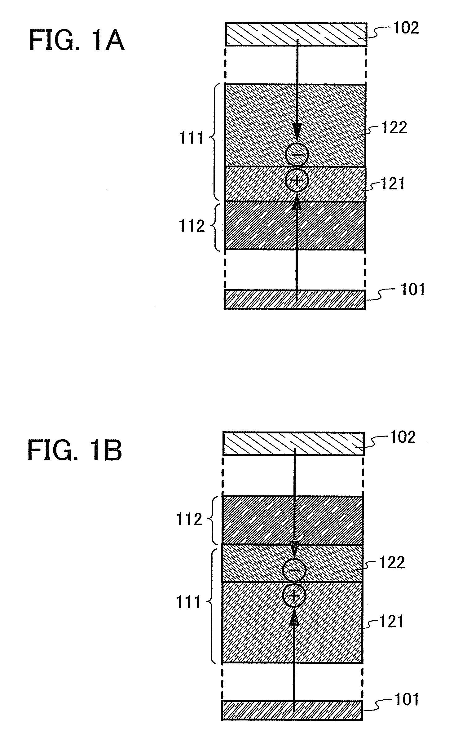
[0087]Embodiment Mode 1 will describe a concept of the present invention. A conceptual view of a light-emitting element of the present invention is shown in FIGS. 1A and 1B.

[0088]FIG. 1A shows one of structures of a light-emitting element of the present invention in which, between an anode 101 and a cathode 102, a first light-emitting layer 111 and a second light-emitting layer 112 which is provided in contact with the anode side of the first light-emitting layer 111 are provided and the first light-emitting layer 111 includes a layer 121 provided on the anode side and a layer 122 provided on the cathode side. Although a hole-injecting layer or a hole-transporting layer may be provided between the anode 101 and the second light-emitting layer 112, it is not necessarily provided; therefore, they are omitted in FIG. 1A. In addition, although an electron-injecting layer or an electron-transporting layer may be provided between the cathode 102 and the first light-emitting layer 111, it ...

embodiment mode 2

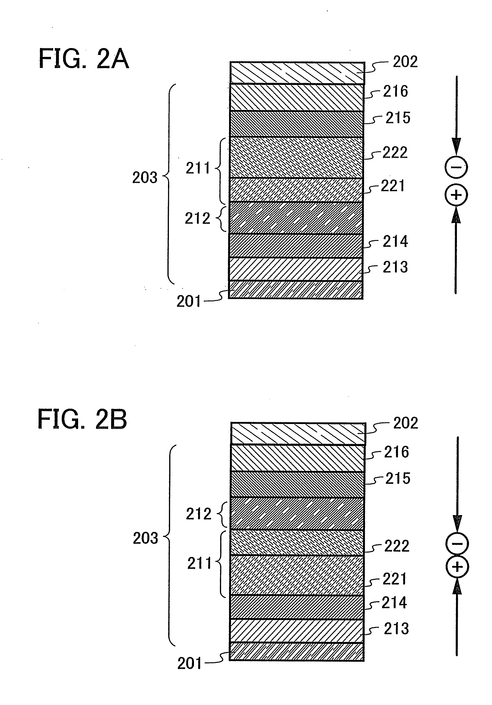
[0106]Embodiment Mode 2 will describe a specific structure of the light-emitting element of the present invention which is described in FIG. 1A with reference to FIG. 2A.

[0107]FIG. 2A is a view schematically showing an element structure of the light-emitting element of the present invention. A layer 203 containing a light-emitting substance is provided between an anode 201 and a cathode 202, and the layer 203 containing a light-emitting substance includes at least a first light-emitting layer 211 and a second light-emitting layer 212 which is provided in contact with the anode side of the first light-emitting layer 211. The first light-emitting layer 211 includes a layer 221 provided on the anode side and a layer 222 provided on the cathode side.

[0108]Note that in the light-emitting element in Embodiment Mode 2, a hole-injecting layer 213 and a hole-transporting layer 214 are provided between the anode 201 and the second light-emitting layer 212. In addition, an electron-transportin...

embodiment mode 3

[0164]Embodiment Mode 3 will describe a specific structure of the light-emitting element of the present invention which is described in FIG. 1B with reference to FIG. 2B.

[0165]FIG. 2B is a view schematically showing an element structure of the light-emitting element of the present invention. The layer 203 containing a light-emitting substance is provided between the anode 201 and the cathode 202, and the layer 203 containing a light-emitting substance includes at least the first light-emitting layer 211 and the second light-emitting layer 212 which is provided in contact with the cathode side of the first light-emitting layer 211. The first light-emitting layer 211 includes the layer 221 provided on the anode side and the layer 222 provided on the cathode side.

[0166]Note that in the light-emitting element in Embodiment Mode 3, the hole-injecting layer 213 and the hole-transporting layer 214 are provided between the anode 201 and the first light-emitting layer 211. In addition, the e...


PUM


Abstract

To provide a long lifetime light-emitting element, in particular, to provide a long lifetime white light-emitting element, and to provide a light-emitting element having high luminous efficiency, in particular, to provide a white light-emitting element having high luminous efficiency. In a light-emitting element having, between an anode and a cathode, a first light-emitting layer containing a first light-emitting substance and a second light-emitting layer containing a second light-emitting substance which is provided to be in contact with the first light-emitting layer, the first light-emitting layer is divided into a layer provided on the anode side and a layer provided on the cathode side. At this time, a host material having a hole-transporting property is used for the layer provided on the anode side, and a host material having an electron-transporting property is used for the layer provided on the cathode side.

Description

BACKGROUND OF THE INVENTION[0001]1. Field of the Invention[0002]The present invention relates to a current-excitation light-emitting element. In addition, the present invention relates to a light-emitting device and an electronic device having the light-emitting element.[0003]2. Description of the Related Art[0004]In recent years, research and development have been actively conducted on light-emitting elements using electroluminescence. In a basic structure of such a light-emitting element, a layer containing a light-emitting substance is interposed between a pair of electrodes. By applying voltage to this element, light emission from the light-emitting substance can be obtained.[0005]Light-emitting elements using electroluminescence are broadly classified according to whether the light-emitting substance is an organic compound or an inorganic compound.[0006]In the case where an organic compound is used for the light-emitting substance, by applying voltage to a light-emitting elemen...

Claims


Application Information

Patent Timeline
Patent Type & Authority Applications(United States)
IPC IPC(8): H01J1/62H01L51/30H01L51/50H05B33/12
CPCC09K11/06H01L51/0052H01L51/0058Y02B20/181H01L51/0072H01L51/5036H01L51/006Y02B20/00H10K85/626H10K85/633H10K85/615H10K85/6572H10K50/125H05B33/14H10K50/00
Inventor USHIKUBO, TAKAHIROSEO, SATOSHI
Owner SEMICON ENERGY LAB CO LTD
Why Eureka
Try Eureka