Oleds for micro transfer printing

Active Publication Date: 2017-03-30
X DISPLAY CO TECH LTD
View PDF7 Cites 52 Cited by
  • Summary
  • Abstract
  • Description
  • Claims
  • Application Information

AI Technical Summary

Benefits of technology

[0008]The present invention provides structures, devices and methods for organic light-emitting diodes and color displays that require fewer or no shadow masks for evaporative deposition of organic materials. The organic light-emitting diode structures can be micro transfer printed and organic light-emitting diode structures that each emit different colors of light can be separately constructed on separate source substrates, released from the source substrate, and micro transfer printed to a destination display substrate. The organic light-emitting diode structures and methods mitigate the problems encountered with repeated use of fine metal shadow masks, such as alignment to a common display substrate and damage to organic materials deposited on the display substrate.

Problems solved by technology

Moreover, in an embodiment, the use of fine metal shadow masks is unnecessary for patterning evaporated organic materials.

Method used


Image

  • Oleds for micro transfer printing
  • Oleds for micro transfer printing
  • Oleds for micro transfer printing

Examples


Embodiment Construction

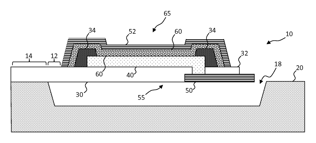
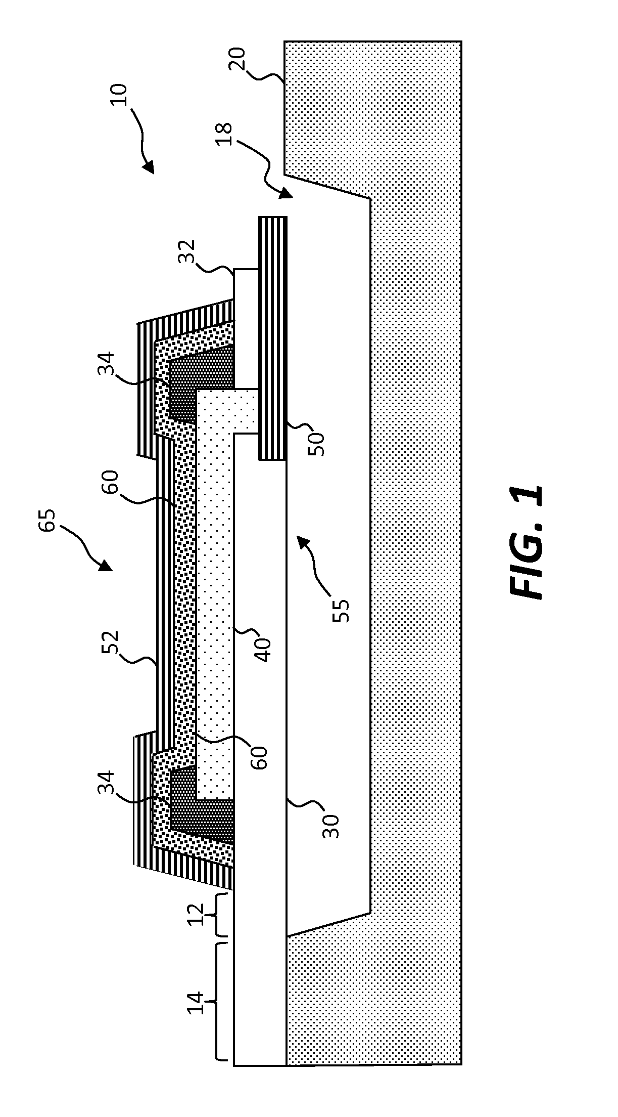
[0091]Referring to the cross section of FIG. 1, in an embodiment of the present invention an organic light-emitting diode (OLED) structure 10 includes an organic light-emitting diode 65 having a first electrode 55, one or more layers of organic material 60 disposed on at least a portion of the first electrode 55, and a second electrode 52 disposed on at least a portion of the one or more layers of organic material 60. The OLED structure 10 includes at least a portion of a tether 12 extending from a periphery of the organic light-emitting diode 65. In an embodiment, the OLED structure 10 is a micro transfer printable OLED 65.

[0092]In the embodiment of FIG. 1, the first electrode 55 includes a first electrode portion 50 and a transparent electrode 40 that is in electrical contact with the first electrode portion 50. The first electrode portion 50 can be opaque, for example made of an electrically conductive metal such as aluminum, silver, gold, tungsten, or titanium. The transparent e...


PUM


Abstract

An organic light-emitting diode (OLED) structure includes an organic light-emitting diode having a first electrode, one or more layers of organic material disposed on at least a portion of the first electrode, and a second electrode disposed on at least a portion of the one or more layers of organic material. At least a portion of a tether extending from a periphery of the organic light-emitting diode. The organic light-emitting diodes can be printable organic light-emitting diode structures that are micro transfer printed over a display substrate to form a display.

Description

FIELD OF THE INVENTION[0001]The present invention relates to organic light-emitting diode (OLED) displays and to micro transfer printing.BACKGROUND OF THE INVENTION[0002]Flat-panel displays are widely used in conjunction with computing devices, in portable devices, and for entertainment devices such as televisions. Such displays typically employ a plurality of pixels distributed over a display substrate to display images, graphics, or text. In a color display, each pixel includes light emitters that emit light of different colors, such as red, green, and blue. For example, liquid crystal displays (LCDs) employ liquid crystals to block or transmit light from a backlight behind the liquid crystals and organic light-emitting diode (OLED) displays rely on passing current through a layer of organic material that glows in response to the current. Displays using inorganic light emitting diodes (LEDs) are also in widespread use for outdoor signage and have been demonstrated in a 55-inch tel...

Claims


Application Information

Patent Timeline
Patent Type & Authority Applications(United States)
IPC IPC(8): H01L51/00H01L27/32H01L51/56H01L51/52
CPCH01L51/0013H01L51/5206H01L27/3206H01L51/5253H01L2227/323H01L51/0023H01L51/5221H01L27/3225H01L51/56H01L2224/24H10K71/80H10K50/00H10K71/00H10K71/18H10K50/81H10K50/82H10K50/844H10K59/00H10K59/30H10K71/621H10K59/1201
Inventor BOWER, CHRISTOPHERMEITL, MATTHEWCOK, RONALD S.
Owner X DISPLAY CO TECH LTD
Why Eureka
Try Eureka