Touch device

a technology of touch and shielding esd, which is applied in the direction of semiconductor devices, instruments, computing, etc., can solve the problems of prone damage of the gate driving circuit and the inability to dispose of the comprehensive transparent conductive layer for shielding esd on the outer surface, so as to achieve the effect of improving the gate driving circui

Active Publication Date: 2017-04-27
INNOLUX CORP
View PDF0 Cites 13 Cited by
  • Summary
  • Abstract
  • Description
  • Claims
  • Application Information

AI Technical Summary

Benefits of technology

[0007]The disclosure is directed to a touch device, which is capable of effectively improving the gate driving circuit from damage caused by ESD.

Problems solved by technology

Therefore, the gate driving circuit is prone to damage caused by Electrostatic Discharge (ESD).
Because the in-cell touch display device has a touch electrode of in-cell type, it is impossible to dispose the comprehensive transparent conductive layer for shielding ESD on the outer surface of the color filter substrate since electronic properties of elements and the touch function of the touch electrode may be affected by doing so.

Method used


Image

  • Touch device
  • Touch device
  • Touch device

Examples


Embodiment Construction

[0037]Reference will now be made in detail to the present embodiments of the disclosure, examples of which are illustrated in the accompanying drawings. Wherever possible, the same reference numbers are used in the drawings and the description to refer to the same or like parts.

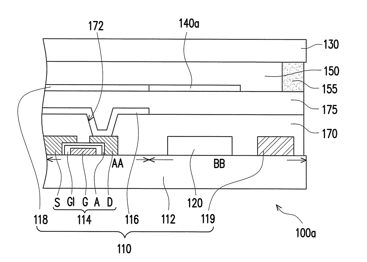
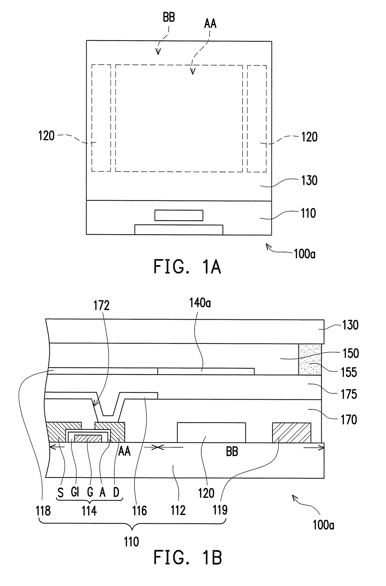
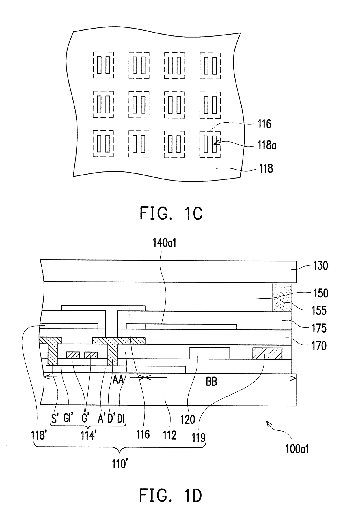
[0038]FIG. 1A illustrates a top view of a touch device according to an embodiment of the disclosure. FIG. 1B illustrates a partial cross-sectional view of the touch device of FIG. 1A. For descriptive convenience, illustration of some elements is omitted in FIG. 1A and FIG. 1B. Referring to FIG. 1A and FIG. 1B together, in the present embodiment, a touch device 100a includes an array substrate 110, at least one gate driving circuit 120 (two of which are schematically illustrated in FIG. 1A), an opposite substrate 130 and a shielding pattern 140a. The array substrate 110 includes a display region AA and a peripheral region BB connecting the display region AA. In another embodiment, the peripheral area BB may su...


PUM


Abstract

A touch device including an array substrate, at least one gate driving circuit, an opposite substrate and a shielding pattern is provided. The array substrate has a display region and a peripheral region connecting to the display region. The gate driving circuit is disposed on the array substrate and located in the peripheral region. The opposite substrate is disposed opposite to the array substrate. The shielding pattern is disposed between the array substrate and the opposite substrate. The shielding pattern projected on the array substrate is formed a first projection, the gate driving circuit projected on the array substrate is formed a second projection, the first projection at least partially overlaps with the second projection.

Description

CROSS-REFERENCE TO RELATED APPLICATION[0001]This application claims the priority benefits of U.S. provisional application Ser. No. 62 / 245,299, filed on Oct. 23, 2015 and Taiwan application serial no. 105110692, filed on Apr. 6, 2016. The entirety of each of the above-mentioned patent applications is hereby incorporated by reference herein and made a part of this specification.BACKGROUND[0002]1. Field of the Invention[0003]The disclosure relates to a touch device.[0004]2. Description of Related Art[0005]In panel design, a technique that directly fabricates a gate driving circuit on an array substrate to replace an external driving chip is known as Gate drive on Array (GOA) technique. In the display devices of In-Plane Switching (IPS) type or Fringe Field Switching (FFS), the gate driving circuit is usually disposed in a peripheral region of the array substrate without any shielding elements disposed thereon. Therefore, the gate driving circuit is prone to damage caused by Electrostat...

Claims


Application Information

Patent Timeline
Patent Type & Authority Applications(United States)
IPC IPC(8): G06F3/044H01L27/02G06F3/041
CPCG06F3/044H01L27/1214G06F3/0416H01L27/0292G06F2203/04107G06F2203/04103G02F2201/123G02F2201/121G02F1/134309G02F1/136204G02F1/13338G02F1/133345G02F1/1339G02F1/133514G02F1/13439H01L27/323H01L27/3272H01L27/3262G06F3/0412G02F1/13454H01L29/78633H01L27/124G06F3/0445H10K59/40H10K59/126H10K59/1213
Inventor WU, CHENG-MIN
Owner INNOLUX CORP
Why Eureka
Try Eureka