Supercharge Your Innovation With Domain-Expert AI Agents!

Manufacturing method of array substrate, trnaslucent passivation film and liquid crystal display panel

Inactive Publication Date: 2017-09-14
TCL CHINA STAR OPTOELECTRONICS TECH CO LTD
View PDF4 Cites 1 Cited by
  • Summary
  • Abstract
  • Description
  • Claims
  • Application Information

AI Technical Summary

Benefits of technology

This patent is about a method for making an array substrate, a translucent passivation film, and a liquid crystal display panel. The method aims to reduce bumps on the top surface of the passivation film and improve the light transmission rate of the display panel. In simple terms, this patent aims to make the display panel more efficient and smooth.

Problems solved by technology

In the conventional manufacturing process, the passivation film is formed by sputtering at a temperature which is higher than 285° C. However, the topology of the top surface of the passivation layer would be bumpy due to the high activity of the passivation material while the high temperature process.

Method used


Image

  • Manufacturing method of array substrate, trnaslucent passivation film and liquid crystal display panel
  • Manufacturing method of array substrate, trnaslucent passivation film and liquid crystal display panel
  • Manufacturing method of array substrate, trnaslucent passivation film and liquid crystal display panel

Examples


Embodiment Construction

[0027]The present disclosure will now be described more specifically with reference to the following embodiments. It is to be noted that the following descriptions of embodiments are presented herein for purpose of illustration and description only. It is not intended to be exhaustive or to be limited to the precise form disclosed.

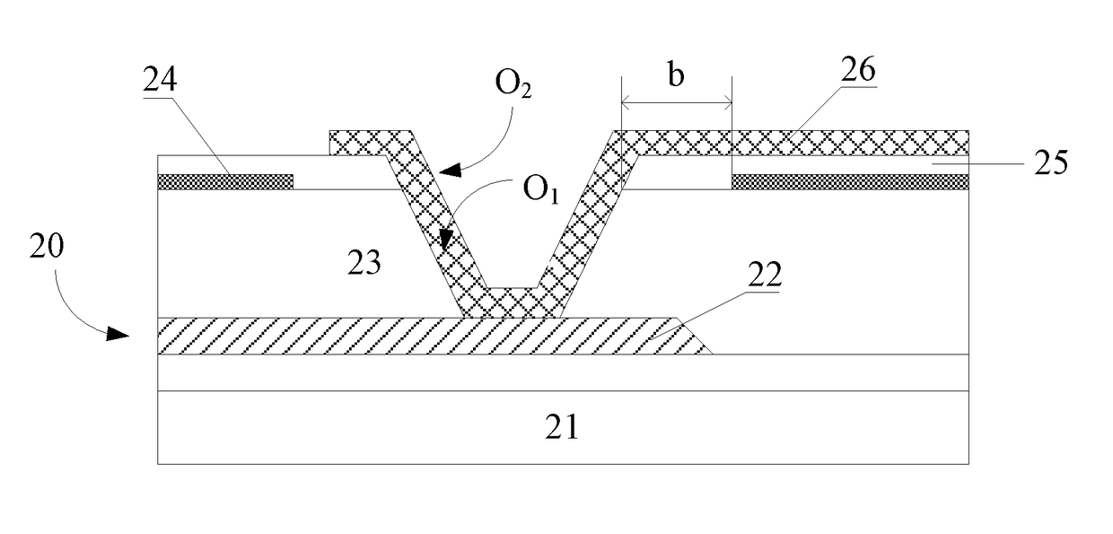
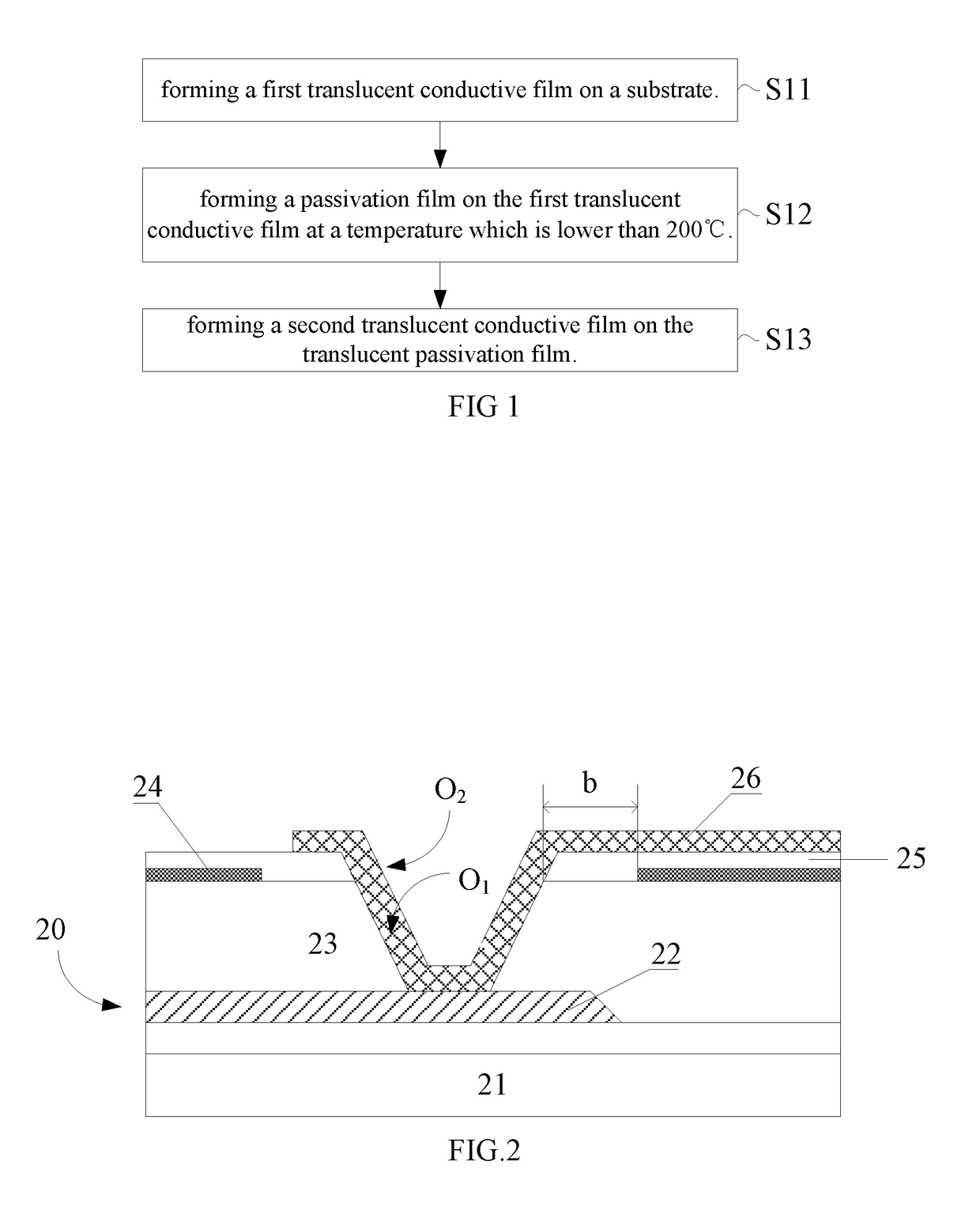
[0028]FIG. 1 is the schematic of manufacturing flow of an array substrate of one embodiment of the present disclosure. This embodiment is to manufacture a structure with three films, which includes a first translucent conductive film, a passivation film, and a second translucent film. With reference to FIG. 1, the manufacturing process comprises:

[0029]S11: forming a first translucent conductive film on a substrate.

[0030]S12: forming a passivation film on the first translucent conductive film at a temperature which is lower than 200° C.

[0031]S13: forming a second translucent conductive film on the translucent passivation film.

[0032]The materials of the firs...


PUM


Abstract

This disclosure discloses a method of manufacturing an array substrate. The method includes forming a first translucent conductive film on a substrate, forming a translucent passivation film on the first translucent conductive film at a temperature lower than 200° C.; and forming a second translucent conductive film on the translucent passivation film. This disclosure also discloses a method of manufacturing a translucent passivation film and a liquid crystal display panel. The particle-like bumps would be reduced and the light transmission rate of the liquid crystal display panel would be improved.

Description

TECHNICAL FIELD[0001]This disclosure is related to the liquid crystal display panel, especially related to a manufacturing method of an array substrate, a translucent passivation film and a liquid crystal display panelDESCRIPTION OF RELATED ART[0002]In the Fringe Field Switching (FFS) type of LCD panel, there are three thin films on an array substrate. The three thin films are a common electrode, a passivation layer and a pixel electrode accordingly. In the conventional manufacturing process, the passivation film is formed by sputtering at a temperature which is higher than 285° C. However, the topology of the top surface of the passivation layer would be bumpy due to the high activity of the passivation material while the high temperature process. The light transmission ratio would be reduced.SUMMARY[0003]To solve the issues mentioned above, the embodiments of the present disclosure provide a manufacturing method of an array substrate, a translucent passivation film and a liquid cr...

Claims


Application Information

Patent Timeline
IPC IPC(8): G02F1/1333G02F1/1362G02F1/1343
CPCG02F1/133345G02F1/13439G02F1/136227G02F1/1368G02F2201/123G02F2001/134372G02F2201/121G02F1/1333G02F1/134363G02F1/134372
Inventor ZHAO, YANG
Owner TCL CHINA STAR OPTOELECTRONICS TECH CO LTD
Features
  • R&D
  • Intellectual Property
  • Life Sciences
  • Materials
  • Tech Scout
  • Unparalleled Data Quality
  • Higher Quality Content
  • 60% Fewer Hallucinations
Learn More