Tiled display panel and tiled display device

a display device and display panel technology, applied in the field of display technology, can solve problems such as serious affecting the display

Active Publication Date: 2018-02-22
BOE TECH GRP CO LTD +1
View PDF4 Cites 29 Cited by
  • Summary
  • Abstract
  • Description
  • Claims
  • Application Information

AI Technical Summary

Benefits of technology

[0051]In summary, in the tiled display panel and the tiled display device according to the embodiments of the present disclosure, by means of providing the first optical element and the second optical element in the display areas and providing the reflective element in the splice region, it can direct the light from the display areas to the splice area and allow it to be emitted from the splice area, therefore the brightness difference between the display areas and the splice area can be reduced, and an image can be displayed on the splice area, thereby improving the display effect of the tiled display panel and the tiled display device.
[0025]The drawings described herein are intended to illustrate the selected embodiments in the present disclosure, but are not intended to be representative of all possible embodiments, and are not intended to limit the scope of the present disclosure. In the drawings:

Problems solved by technology

However, since each sub-display panel includes opaque frame sealing glue and an opaque border, there is an area that cannot display between adjacent sub-display panels, that is a so-called splice gap or splice area, which seriously affects display effect.

Method used


Image

  • Tiled display panel and tiled display device
  • Tiled display panel and tiled display device
  • Tiled display panel and tiled display device

Examples


Embodiment Construction

[0030]Exemplary embodiments will now be described in further detail with reference to the accompanying drawings.

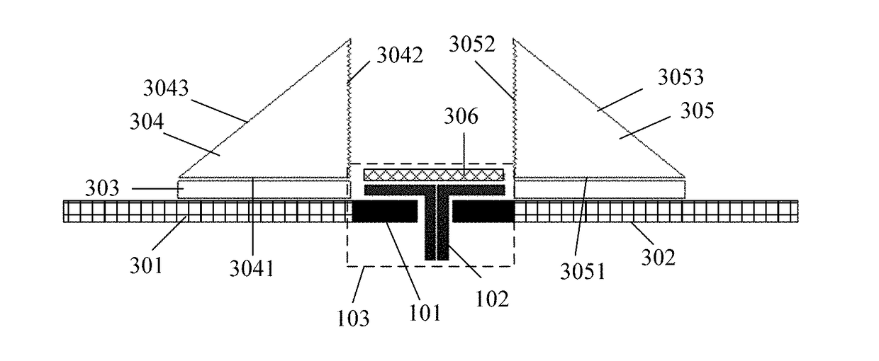
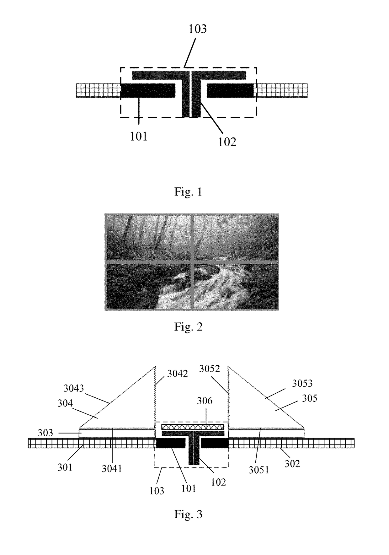
[0031]FIG. 1 is a schematic view showing a splice area between two adjacent sub-display panels. As shown in FIG. 1, due to the presence of frame sealing glue 101 and a border 102 of each sub-display panel, there is an opaque splice area 103 between two adjacent sub-display panels when they are spliced. Since the splice area is not light-transmitted and cannot achieve an image display, a relatively significantly dark area (see FIG. 2) will appear in the splice area when a large format display is implemented, which will seriously affect the display effect. In order to reduce a width of the splice area, various efforts has been made and it has seen some achievements. The width of the splice area has been reduced from 5.9 mm to less than 2 mm. However, due to the presence of the frame sealing glue in a liquid crystal display panel, the splice area cannot be fundamentally elimi...


PUM

PropertyMeasurementUnit
widthaaaaaaaaaa
widthaaaaaaaaaa
areaaaaaaaaaaa

Abstract

A tiled display panel and a tiled display device are disclosed. The tiled display panel includes: at least first and second adjacent display areas; a splice area disposed between the first and second adjacent display areas; a first optical element and a second optical element respectively disposed on the first and second display areas and located on two sides of the splice area; and a reflective element disposed on the splice area. Each of the first optical element and the second optical element is configured to direct at least a portion of light emitted from its respective display area to the reflective element, such that the at least a portion of light is reflected by the reflective element and then emitted out from the splice area.

Description

CROSS-REFERENCE TO RELATED APPLICATION[0001]This application claims the benefit of Chinese Patent Application No. 201610683876.X filed on Aug. 18, 2016 in the State Intellectual Property Office of China, the disclosure of which is incorporated in its entirety herein by reference.BACKGROUNDTechnical Field[0002]Embodiments of the present disclosure relate to a field of display technology, and more particularly, to a tiled display panel and a tiled display device.Description of the Related Art[0003]With the rapid development of display technology, LFD (large format display) technology is more and more popular. Tiled display technology becomes one of the main ways to achieve a large size display. Since a LCD panel has a lot of advantages, such as high resolution, large viewing angle, low power consumption, etc., the existing tiled screen usually uses a number of LCD panels as sub-display panels and splices them. However, since each sub-display panel includes opaque frame sealing glue an...

Claims


Application Information

Patent Timeline
Patent Type & Authority Applications(United States)
IPC IPC(8): G02B17/08G02B5/04G02B5/02G02F1/1333
CPCG02B17/086G02B5/04G02B5/0231G02F1/13336G02B5/0226G09F9/35G02F1/133524
Inventor JIA, LILIZHOU, HAOHU, WEIHAOZHANG, LIANGZHANG, YU
Owner BOE TECH GRP CO LTD
Why Eureka
Try Eureka