Active matrix type display device and drive control circuit used in the same

a display device and active matrix technology, applied in the direction of instruments, static indicating devices, etc., can solve the problems of parasitic capacitance, degrading image quality, and affecting the display quality, and achieve the effect of high display quality

Active Publication Date: 2014-03-25
SHARP KK
View PDF24 Cites 5 Cited by
  • Summary
  • Abstract
  • Description
  • Claims
  • Application Information

AI Technical Summary

Benefits of technology

[0047]As stated above, according to the present invention, data lines corresponding to pixels of a color with a contribution to brightness smaller than a contribution of at least another color among the three colors are connected first and last with the corresponding output signal line of the data line drive circuit during one horizontal period, and therefore a difference in the brightness between the first written pixel and the last written pixel can be made small. As a result, an active matrix display device having a high display quality can be provided.

Problems solved by technology

The manufacturing cost of such an active matrix display device including TFTs may be higher than that of a display device without switching elements.
In the configuration of FIG. 14, however, since the driving order of the grouped data lines DLs is fixed to an arrangement order of the data lines DLs that is in accordance with the scanning direction, there is a problem of a display unevenness in a stripe pattern as described below, thus degrading an image quality.
In the case of TFTs made of amorphous silicon, the ON resistance reaches a several mega Ω, and therefore even a parasitic capacitance cannot be ignored.
. . (group b) of two data lines DLs forming a group, and therefore a practically sufficient image quality cannot be obtained.
Furthermore, in the case of a smaller voltage amplitude than the above, a visual variation will increase more, and therefore the influence thereof cannot be ignored.

Method used


Image

  • Active matrix type display device and drive control circuit used in the same
  • Active matrix type display device and drive control circuit used in the same
  • Active matrix type display device and drive control circuit used in the same

Examples


embodiment 1

[0087][Embodiment 1]

[0088]Referring now to FIG. 1 to FIG. 11, one embodiment of the present invention will be described below.

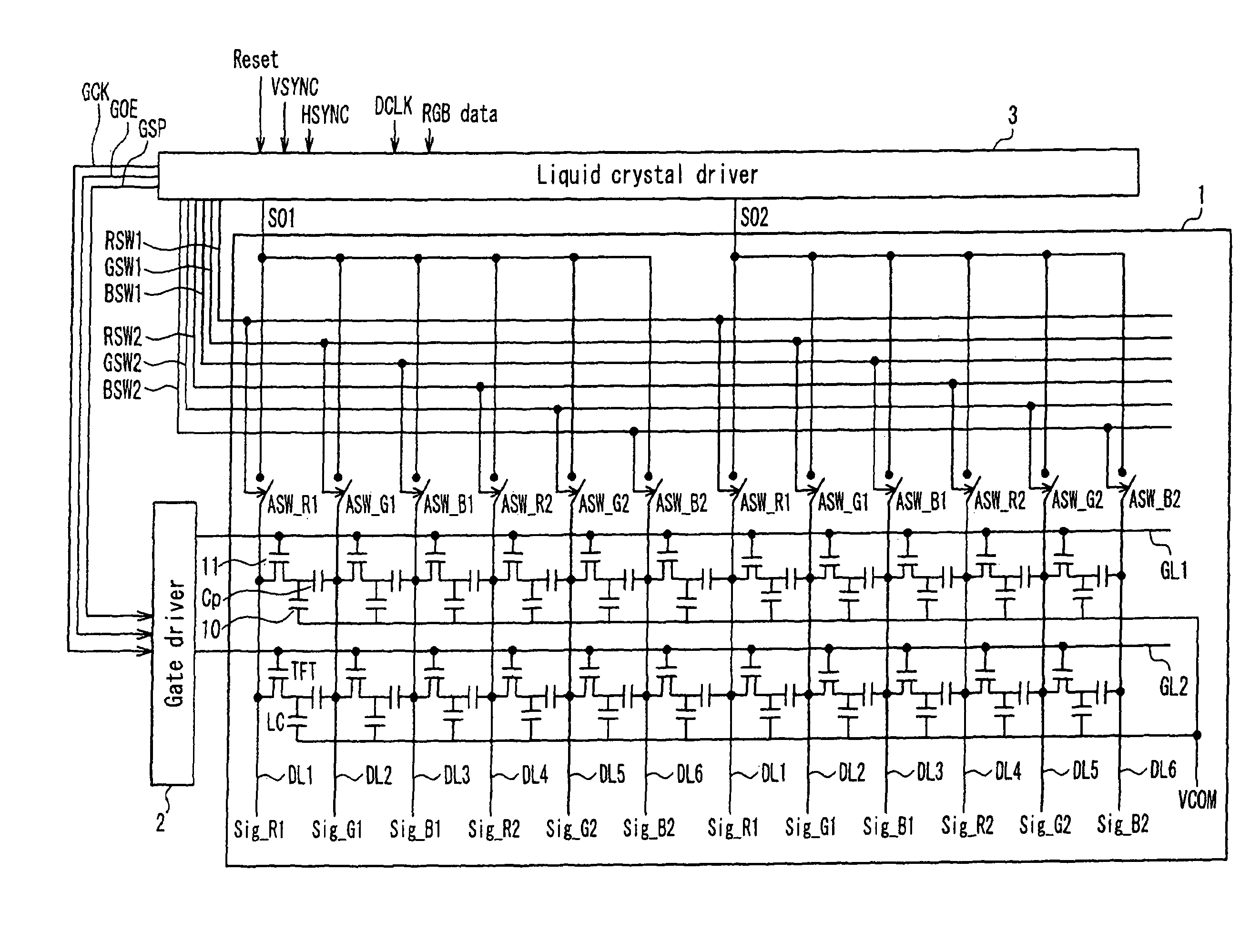
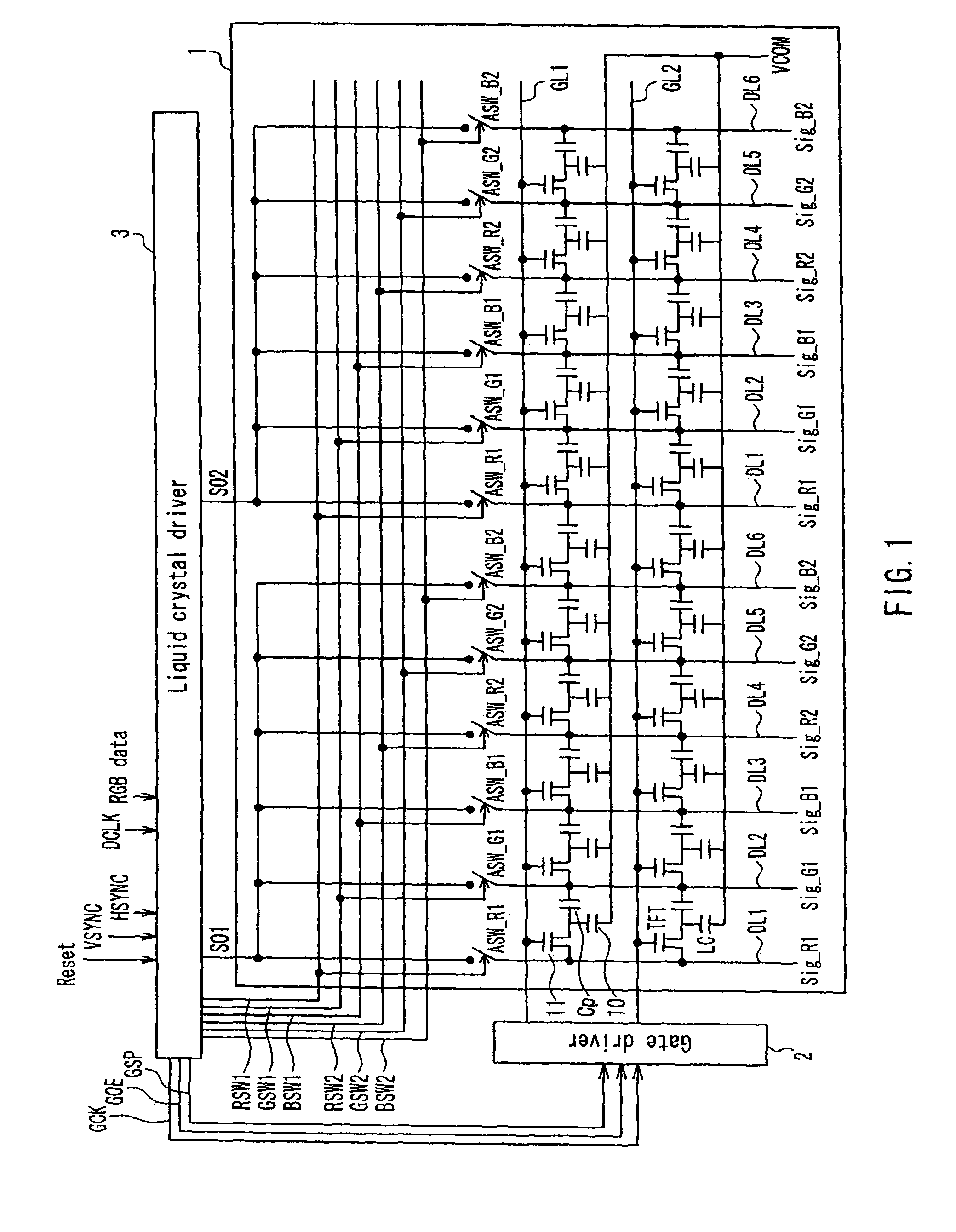
[0089]FIG. 1 is an equivalent circuit diagram illustrating the major configuration of an active matrix liquid crystal display device in accordance with the present embodiment. As shown in FIG. 1, the liquid crystal display device of the present embodiment mainly includes a liquid crystal panel 1, a gate driver 2 and a liquid crystal driver 3 (drive control circuit).

[0090]Although not illustrated, the liquid crystal panel 1 includes a matrix substrate and an opposing substrate that are in parallel and opposed to each other with a space of a predetermined distance therebetween, the space being filled with liquid crystals.

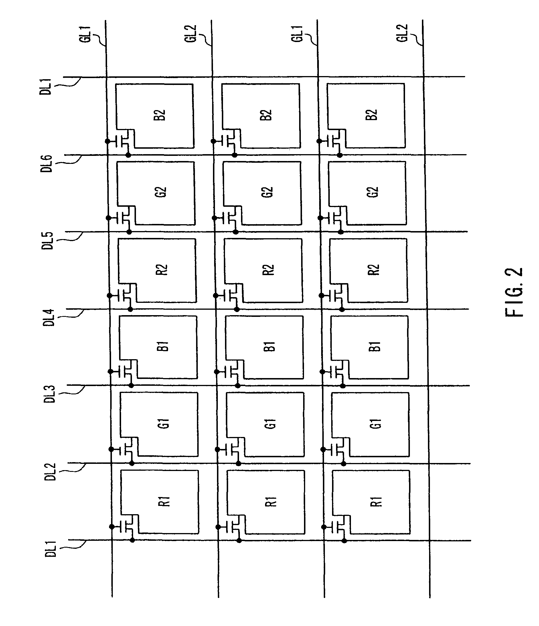
[0091]The matrix substrate is provided with parallel N data lines DL1 to DLN and a plurality of parallel gate lines GL1 to GLM crossing the data lines DLs, and at each of the intersections of these data lines DLs and the gate lines GLs, a pixel...

embodiment 2

[0129](Embodiment 2)

[0130]Referring now to FIG. 12 to FIG. 13, another embodiment of the present invention will be described below. In the following description, the same reference numerals are assigned to the elements having similar functions to those described in Embodiment 1, and their detailed explanations are not repeated.

[0131]FIG. 12 is an equivalent circuit diagram illustrating the major configuration of an active matrix liquid crystal display device in accordance with the present embodiment. As shown in FIG. 12, the liquid crystal display device of the present embodiment mainly includes a liquid crystal panel 21, a gate driver 2 and a liquid crystal driver 3.

[0132]The liquid crystal panel 21 includes a three primary colored (RGB) color filter layer forming a delta arrangement as shown in FIG. 13, and the liquid crystal panel 21 is different from the liquid crystal panel 1 of Embodiment 1 in that data lines DLs, pixel TFTs, pixel electrodes and the like are arranged correspo...


PUM


Abstract

In an active matrix display device including pixels of three colors having a stripe arrangement or a delta arrangement, n (n denotes a multiple of 3 that is 6 or larger) adjacent data lines form one group and are connected to a source signal output line. The ON / OFF of a selection switch provided for each data line is controlled so that, among the n data lines forming one group, data lines corresponding to pixels of a color with a contribution to brightness smaller than a contribution of at least another color among the three colors are connected first and last with the source signal output line during one horizontal period.

Description

TECHNICAL FIELD[0001]The present invention relates to an active matrix display device such as a liquid crystal display device using thin film transistors (TFTs). More particularly, the present invention relates to an active matrix display device in which a plurality of data lines for transmitting video signals are connected as one unit to an output of a data line drive circuit, and also relates to a drive control circuit used therefor.BACKGROUND ART[0002]In recent years, liquid crystal display devices and electroluminescence (EL) display devices are used widely as flat panel displays. In particular, active matrix display devices having each pixel provided with a switching element have become widespread because of their intrinsic advantages such as high contrast and quick response.[0003]As the switching elements, nonlinear resistance elements and semiconductor elements are used, and among them TFTs formed on a transparent insulation substrate are used because they enable the transmis...

Claims


Application Information

Patent Timeline
Patent Type & Authority Patents(United States)
IPC IPC(8): G09G3/36
CPCG09G2310/027G09G3/3607G09G2310/0251G09G2320/0209G09G3/3688G09G2310/0218G09G2310/0297
Inventor TSUDA, TAKUYASASAGAWA, MAKIINADA, KEN
Owner SHARP KK
Why Eureka
Try Eureka