Image sensor

Active Publication Date: 2018-05-31
SAMSUNG ELECTRONICS CO LTD
View PDF5 Cites 1 Cited by
  • Summary
  • Abstract
  • Description
  • Claims
  • Application Information

AI Technical Summary

Benefits of technology

This patent aims to offer an image sensor that can reduce the impact of noise and accurately determine the voltage of a pixel and a reset.

Problems solved by technology

However, when each pixel of an image sensor includes these multiple photoelectric devices, the images captured by the image sensor may be adversely affected by noise.

Method used


Image

  • Image sensor
  • Image sensor
  • Image sensor

Examples


Embodiment Construction

[0024]Hereinafter, exemplary embodiments of the present inventive concept will be described with reference to the attached drawings.

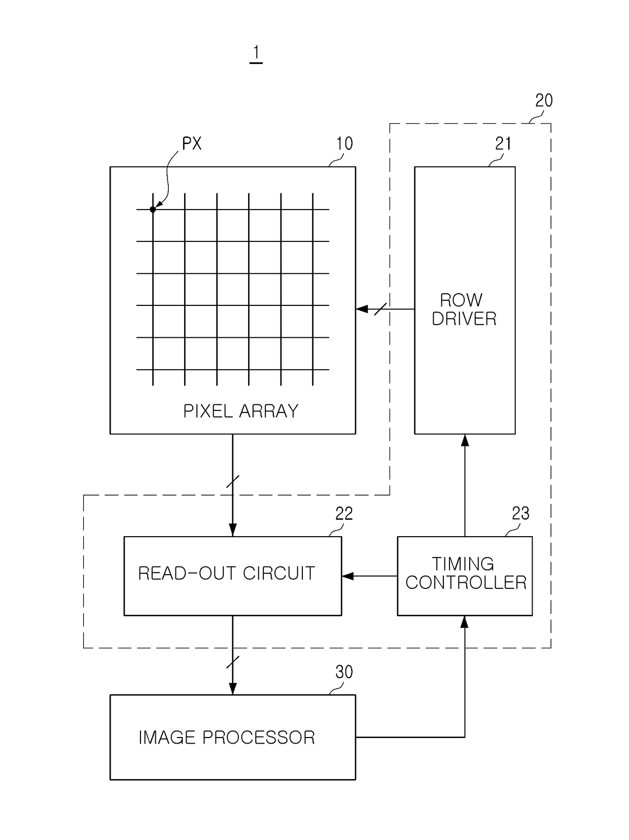
[0025]FIG. 1 is a block diagram of an image processing device according to an exemplary embodiment of the present inventive concept.

[0026]With reference to FIG. 1, an image processing device 1, according to an exemplary embodiment, includes a pixel array 10, a sensor circuit 20, and an image processor 30.

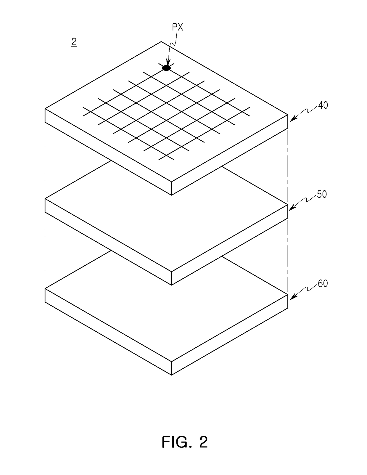
[0027]The pixel array 10 includes a plurality of pixels PX arranged along a plurality of row lines and a plurality of column lines. Each of the plurality of pixels PX includes a photoelectric device, such as a photodiode PD, receiving light and generating an electric charge from the received light. In an exemplary embodiment of the inventive concept, each of the plurality of pixels PX includes two or more photoelectric devices. In an embodiment, the two or more photoelectric devices included in a single pixel PX receive light having different colors and...


PUM


Abstract

An image sensor includes a photoelectric device generating an electric charge from light; a feedback device generating a reset voltage using a predetermined reference voltage; and a pixel circuit generating a pixel voltage using the reset voltage and the electric charge, setting the reset voltage to the reference voltage using the feedback device a first period, and outputting the pixel voltage and the reset voltage during a second period.

Description

CROSS-REFERENCE TO RELATED APPLICATION[0001]This application claims the benefit of priority to Korean Patent Application No. 10-2016-0159662, filed on Nov. 28, 2016 in the Korean Intellectual Property Office, the disclosure of which is incorporated by reference in its entirety herein.BACKGROUND1. Technical Field[0002]The present inventive concept relates to an image sensor.2. Discussion of Related Art[0003]Semiconductor-based image sensors generate electrical signals from received light and may include a pixel array having a plurality of pixels and a circuit driving the pixel array. Semiconductor-based image sensors have been widely used in smartphones, tablet PCs, laptop computers, televisions, and cameras. Each pixel in the pixel area may include multiple photoelectric devices generating an electric charge from light having different colors. However, when each pixel of an image sensor includes these multiple photoelectric devices, the images captured by the image sensor may be adv...

Claims


Application Information

Patent Timeline
IPC IPC(8): H04N5/363H04N5/357H04N5/355H04N5/345H04N9/04H01L27/146
CPCH04N5/363H04N5/3575H04N5/3559H04N5/3452H04N9/045H01L27/14612H01L27/1463H01L27/1461H01L27/14636H01L27/14645H01L27/14634H01L27/14627H01L27/14621H01L27/14609H04N23/10H04N25/76H04N25/616H04N25/65H04N25/709H04N25/77H04N25/713H04N25/766H04N25/75H04N25/59H04N25/441
Inventor KEEL, MIN-SUNKOH, KYOUNGMINHA, SANGHOON
Owner SAMSUNG ELECTRONICS CO LTD
Why Eureka
Try Eureka