Semiconductor inspection jig
a technology of electromagnetic radiation and electromagnetic radiation, applied in the direction of electrical measurement instrument details, measurement devices, instruments, etc., can solve the problems of low mechanical durability of metal patterns, inability to perform inspections, and deterioration of metallic patterns after long-time use, so as to achieve the effect of prolonging the product li
- Summary
- Abstract
- Description
- Claims
- Application Information
AI Technical Summary
Benefits of technology
Problems solved by technology
Method used
Image

Examples
first embodiment
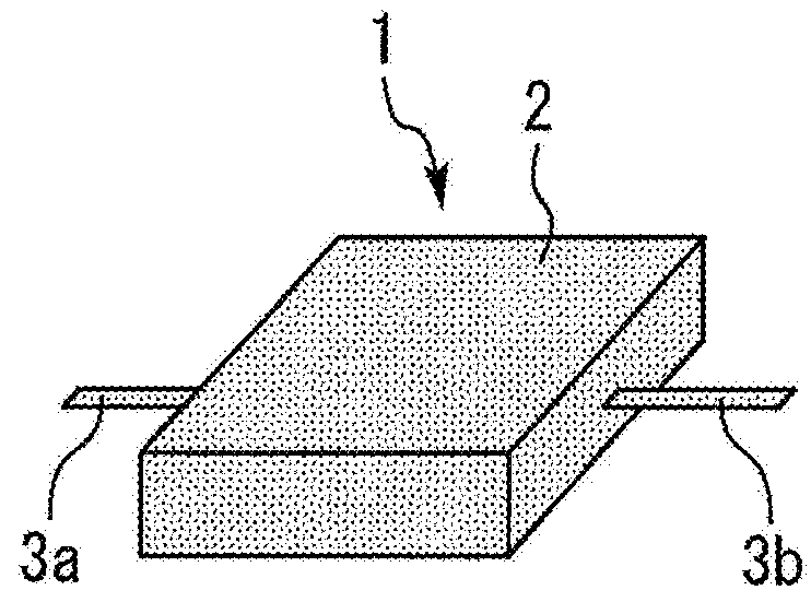
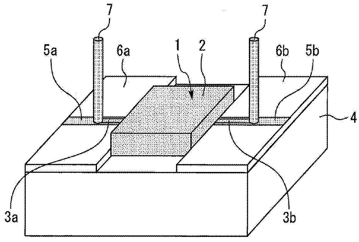
[0018]FIG. 1 is a perspective view illustrating a semiconductor device to be inspected. A semiconductor device 1 is a high-frequency power amplifier that handles high electric power. The semiconductor device 1 includes a body part 2 having a semiconductor chip sealed therein, and leads 3a and 3b which project from the body part 2 in opposite directions. In the body part 2, the leads 3a and 3b are connected to the semiconductor chip. The semiconductor chip is sealed in the body part 2 by, for example, plastic molding. However, the method for sealing the semiconductor chip is not limited to this.
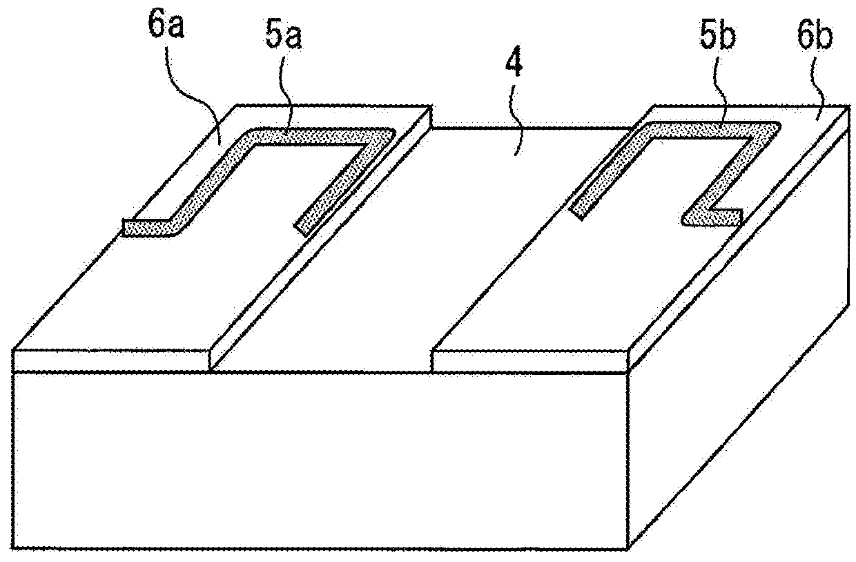
[0019]FIG. 2 is a perspective view illustrating a semiconductor inspection jig according to the first embodiment of the present invention. A base 4 is a mount part on which the semiconductor device 1 is placed. Alumina substrates 6a and 6b including conductive patterns 5a and 5b, respectively, are formed on the base 4. The conductive patterns 5a and 5b are transmission lines for high-frequency...
second embodiment
[0023]FIG. 5 is a perspective view illustrating a semiconductor inspection jig according to a second embodiment of the present invention. The conductive patterns 5a and 5b on the alumina substrates 6a and 6b are not brought into direct contact with the leads 3a and 3b of the semiconductor device 1, which is placed on the base 4, and are spaced apart from each other. A contact sheet 8 is a resin film on which conductive patterns 9a and 9b are formed in the vertical direction with respect to the leads 3a and 3b. The contact sheet 8 is provided with a hole 10 which has a shape that matches the outer diameter size of the body part 2 of the semiconductor device 1.
[0024]FIG. 6 is a perspective view illustrating a state where the inspection of the semiconductor device is performed using the semiconductor inspection jig according to the second embodiment of the present invention. The semiconductor device 1 is placed on the base 4 and the contact sheet 8 is positioned in such a manner that t...
third embodiment
[0026]FIG. 7 is a perspective view illustrating a semiconductor inspection jig according to a third embodiment of the present invention. In this embodiment, lead holding members 11a and 11b having the conductive patterns 9a and 9b formed thereon, respectively, in the vertical direction with respect to the leads 3a and 3b are used instead of the contact sheet 8 of the second embodiment. The other components of the third embodiment are similar to those of the second embodiment.
[0027]FIG. 8 is a perspective view illustrating a state where the inspection of the semiconductor device is performed using the semiconductor inspection jig according to the third embodiment of the present invention. The semiconductor device 1 is placed on the base 4 and the leads 3a and 3b are held by the lead holding members 11a and 11b, respectively. With this structure, the conductive patterns 9a and 9b are brought into direct contact with intermediate parts of the leads 3a and 3b, respectively, without bein...
PUM
 Abstract
Description
Claims
Application Information
 - R&D
- Intellectual Property
- Life Sciences
- Materials
- Tech Scout
- Unparalleled Data Quality
- Higher Quality Content
- 60% Fewer Hallucinations
Browse by: Latest US Patents, China's latest patents, Technical Efficacy Thesaurus, Application Domain, Technology Topic, Popular Technical Reports.
© 2025 PatSnap. All rights reserved.Legal|Privacy policy|Modern Slavery Act Transparency Statement|Sitemap|About US| Contact US: help@patsnap.com