Switch device and storage unit
a technology of switch device and switch device, which is applied in the direction of digital storage, semiconductor devices, instruments, etc., can solve the problems of difficult increase of cross points, and achieve the effect of small and large variation of operation threshold voltage of switch devi
- Summary
- Abstract
- Description
- Claims
- Application Information
AI Technical Summary
Benefits of technology
Problems solved by technology
Method used
Image

Examples
embodiment
1. Embodiment
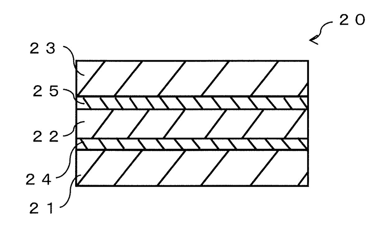
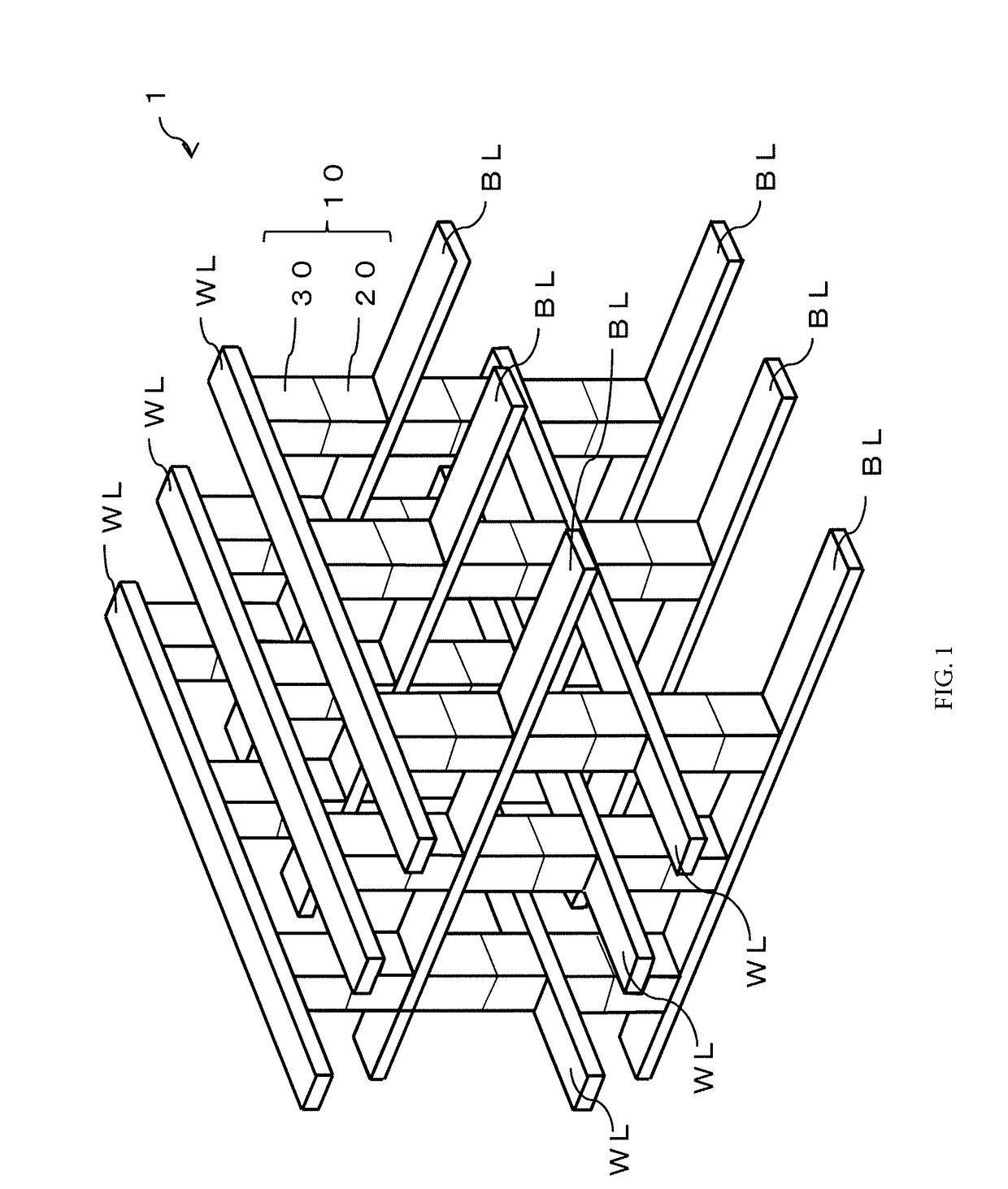
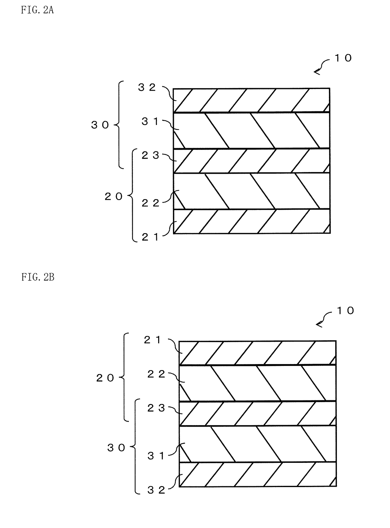
[0053]FIG. 1 is a diagram illustrating a perspective configuration of a memory cell array 1 according to an embodiment of the disclosure. The memory cell array 1 corresponds to a specific example of a “storage unit” of the disclosure. The memory cell array 1 has a so-called cross point array structure, and includes memory cells 10. For example, as illustrated in FIG. 1, each of the memory cells 10 is provided at a position (a cross point) where each of word lines WL and each of bit lines BL face each other. In other words, the memory cell array 1 includes the plurality of word lines WL, the plurality of bit lines BL, and the plurality of memory cells 10 that are disposed at the respective cross points one by one. As described above, the memory cell array 1 of the present embodiment has a three-dimensional structure in which the plurality of memory cells 10 are disposed in plane (two-dimensionally, in an XY plane direction), and are further stacked in a Z axis direction....
experiment 1
[0091]In Experiment 1, five samples (samples 01 to 05) were fabricated. A large number of switch devices 20 were formed on a surface of each of the samples. Each of the samples was formed in the following manner. First, a plurality of MOS transistor circuits and a plurality of first electrodes 21 including TiN were formed on a substrate while being exposed. The surface of the substrate was cleaned through reverse sputtering. Next, a Te target and a B4C target were concurrently sputtered while causing nitrogen to flow into a chamber, to form a BCTeN layer with a thickness of 20 nm on the first electrodes 21 including TiN. Subsequently, a W layer with a thickness of 30 nm was formed on a surface of the BCTeN layer. Thereafter, patterning was performed to form, on the substrate, the large number of switch devices 20 in which the first electrode 21 including TiN, the switch layer 22 configured by BCTeN layer, and the intermediate electrode 23 configured by the W layer were stacked. Heat...
experiment 2
[Experiment 2]
[0097]In Experiment 2, two samples (samples 06 and 07) were fabricated. A large number of switch devices 20 were formed on a surface of each of the samples. Each of the samples was fabricated in the following manner. The sample 06 is first described. A plurality of MOS transistor circuits and a plurality of first electrodes 21 including TiN were formed on a substrate while being exposed. The surface of the substrate was cleaned through reverse sputtering. Thereafter, a SiNx layer was formed through sputtering on the first electrodes 21 including TiN. Thereafter, the sample 06 was taken out from a chamber to the atmosphere once, and the sample 06 was then put in a photolithography process step to form a contact hole on the SiNx layer. Thereafter, the surface of the sample 06 was cleaned through reverse sputtering, and a TiN layer with a thickness of 10 nm was then formed in the contact hole. Subsequently, a BCTeN layer with a thickness of 20 nm was formed on a surface o...
PUM
 Abstract
Description
Claims
Application Information
 - R&D
- Intellectual Property
- Life Sciences
- Materials
- Tech Scout
- Unparalleled Data Quality
- Higher Quality Content
- 60% Fewer Hallucinations
Browse by: Latest US Patents, China's latest patents, Technical Efficacy Thesaurus, Application Domain, Technology Topic, Popular Technical Reports.
© 2025 PatSnap. All rights reserved.Legal|Privacy policy|Modern Slavery Act Transparency Statement|Sitemap|About US| Contact US: help@patsnap.com