Input unit, input method, input system, and input support system
- Summary
- Abstract
- Description
- Claims
- Application Information
AI Technical Summary
Benefits of technology
Problems solved by technology
Method used
Image
Examples
embodiment 1
[0060]In this embodiment, an information terminal and an input unit which are embodiments of the present invention will be described.
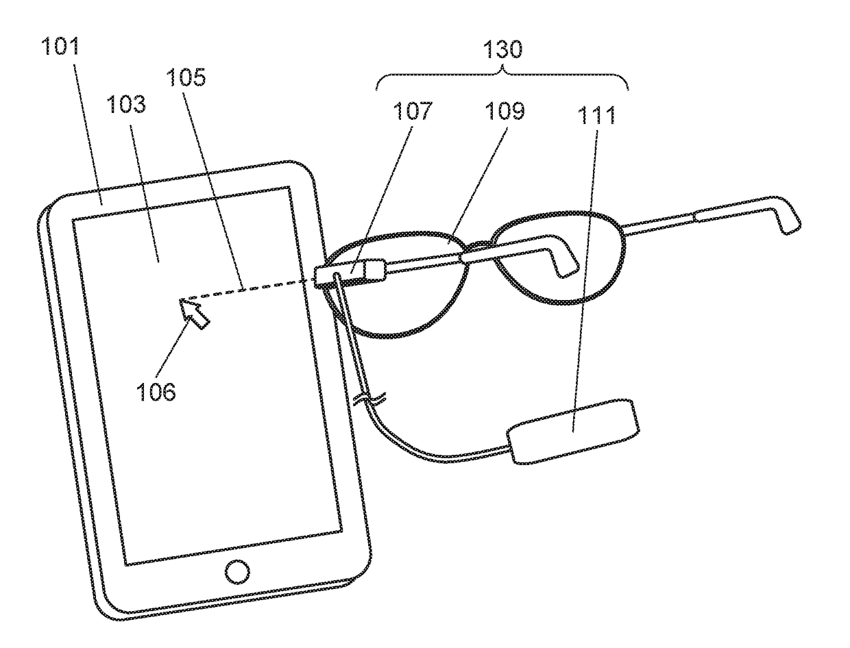
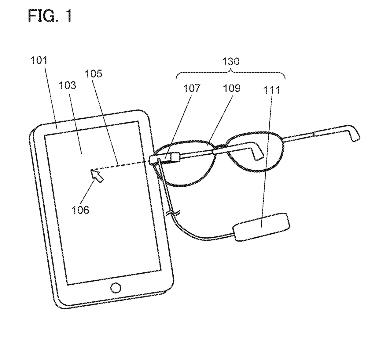
[0061]An information terminal 101 illustrated in FIG. 1 includes a display portion 103. A sensor for detecting a laser light 105 is provided in the display portion. As the sensor for detecting the laser light 105, a photosensor or a photodiode can be used. The sensor can preferably detect the intensity of laser light in a light-receiving portion.
[0062]Note that external light such as light from a usual lighting device and sun light is presumably incident on the display portion 103. To distinguish such external light from light for inputting information to an information terminal, the light for information input preferably has energy higher than the energy of the external light. Laser light is preferably used as the light having high energy.
[0063]For another example, the intensities of the energies of incident light are compared by a plurality of sensor...
embodiment 2
[0133]In this embodiment, a circuit configuration of a display portion of the information terminal that can be used in the present invention is described with reference to FIG. 13 to FIG. 16. In this embodiment, an example of using a photosensor as a sensor included in the display portion is shown. The photosensor detects laser light output from an input unit.
[0134]FIG. 13 illustrates the structure of the display portion. A display panel 150 includes a pixel circuit 151, a display element control circuit 152, and a photosensor control circuit 153.
[0135]The pixel circuit 151 corresponds to the display portion 103 in FIG. 1 and includes a plurality of pixels 154 arranged in a matrix of rows and columns. Each of the pixels 154 includes a display element 155 and a photosensor 156. The photosensor is not necessarily provided for each of the pixels 154, and may be provided for a plurality of pixels. Alternatively, the photosensor may be provided outside the pixels 154.
[0136]A circuit diag...
modification example
[0161]Next, modification examples of the circuit configuration of the photosensor 156 in FIG. 14 and FIG. 15 are described with reference to FIGS. 17A and 17B.
[0162]FIG. 17A illustrates a structure in which the gate of the transistor 205 in FIG. 14 and FIG. 15 is connected to a transistor 250 for controlling the reset operation of the photosensor. Specifically, one of a source and a drain of the transistor 250 is electrically connected to the photosensor reference signal line 213 and the other thereof is electrically connected to the gate of the transistor 205. One electrode of the photodiode 204 is electrically connected to a wiring to which a predetermined potential (e.g., a ground potential) is applied.
[0163]The transistor 250 includes a semiconductor, such as a semiconductor containing silicon, an oxide semiconductor, or a compound semiconductor. There is no limitation on the crystallinity of the semiconductor, and an amorphous semiconductor, a microcrystal semiconductor, a poly...
PUM
 Abstract
Description
Claims
Application Information


