Fabrication of self-aligned gate contacts and source/drain contacts directly above gate electrodes and source/drains

a technology of gate electrodes and self-aligned gate contacts, which is applied in the direction of semiconductor devices, electrical apparatus, semiconductor/solid-state device details, etc., can solve the problems of difficult formation of individual components and electrical contacts

Active Publication Date: 2018-07-26
IBM CORP
View PDF7 Cites 21 Cited by
  • Summary
  • Abstract
  • Description
  • Claims
  • Application Information

AI Technical Summary

Benefits of technology

[0005]A method is provided for forming an active device having self-aligned source/drain contacts and gate contacts. The method includes the steps of forming an active area on a substrate, where the active area includes a device channel; forming two or more gate structures on the device channel; forming a plurality of source/drains on the active area adjacent to the two or more gate structures and device channel; forming a protective layer on the surfaces of the two or more gate structures, plurality of source/drains, and active layer; forming an interlayer dielectric layer on the protective layer; removing a portion of the interlayer dielectric and protective layer to form a plurality of openings, where each opening exposes at least a portion of one of the plurality of source/drains; forming a source/drain contact liner in at least one of the plurality of openings, wherein the protective layer is between the source/drain contact liner and at least one of the two or more gate structures; and forming a source/drain contact fill on the source/drain contact liner.
[0006]A method is provided for forming an active device having self-aligned source/drain contacts and gate contacts. The method includes the steps of forming an active area on a substrate, where the active area includes a device channel; forming two or more gate structures on the device channel, wherein each of the two or more gate structures includes a gate dielectric layer, a conductive gate fill, and a work function layer within a gate sidewall spacer, and the gate dielectric layer, conductive gate fill, and work function layer are covered by a gate structure cap; forming a plurality of source/drains on the active area adjacent to the two or more gate structures and devi

Problems solved by technology

With ever decreasing device dimensions, forming the individu

Method used


Image

  • Fabrication of self-aligned gate contacts and source/drain contacts directly above gate electrodes and source/drains
  • Fabrication of self-aligned gate contacts and source/drain contacts directly above gate electrodes and source/drains
  • Fabrication of self-aligned gate contacts and source/drain contacts directly above gate electrodes and source/drains

Examples


Embodiment Construction

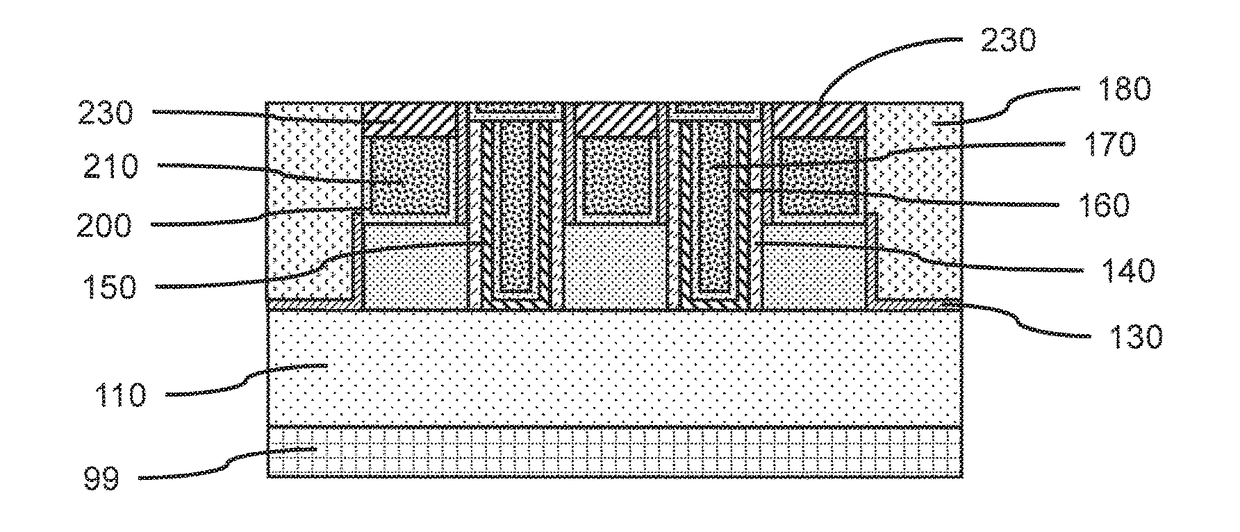
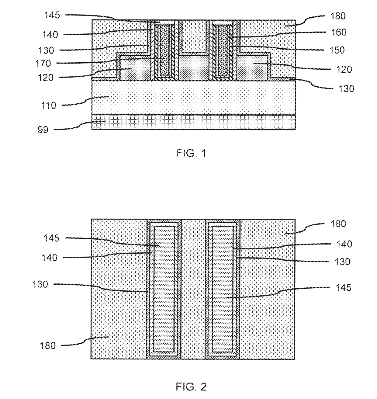
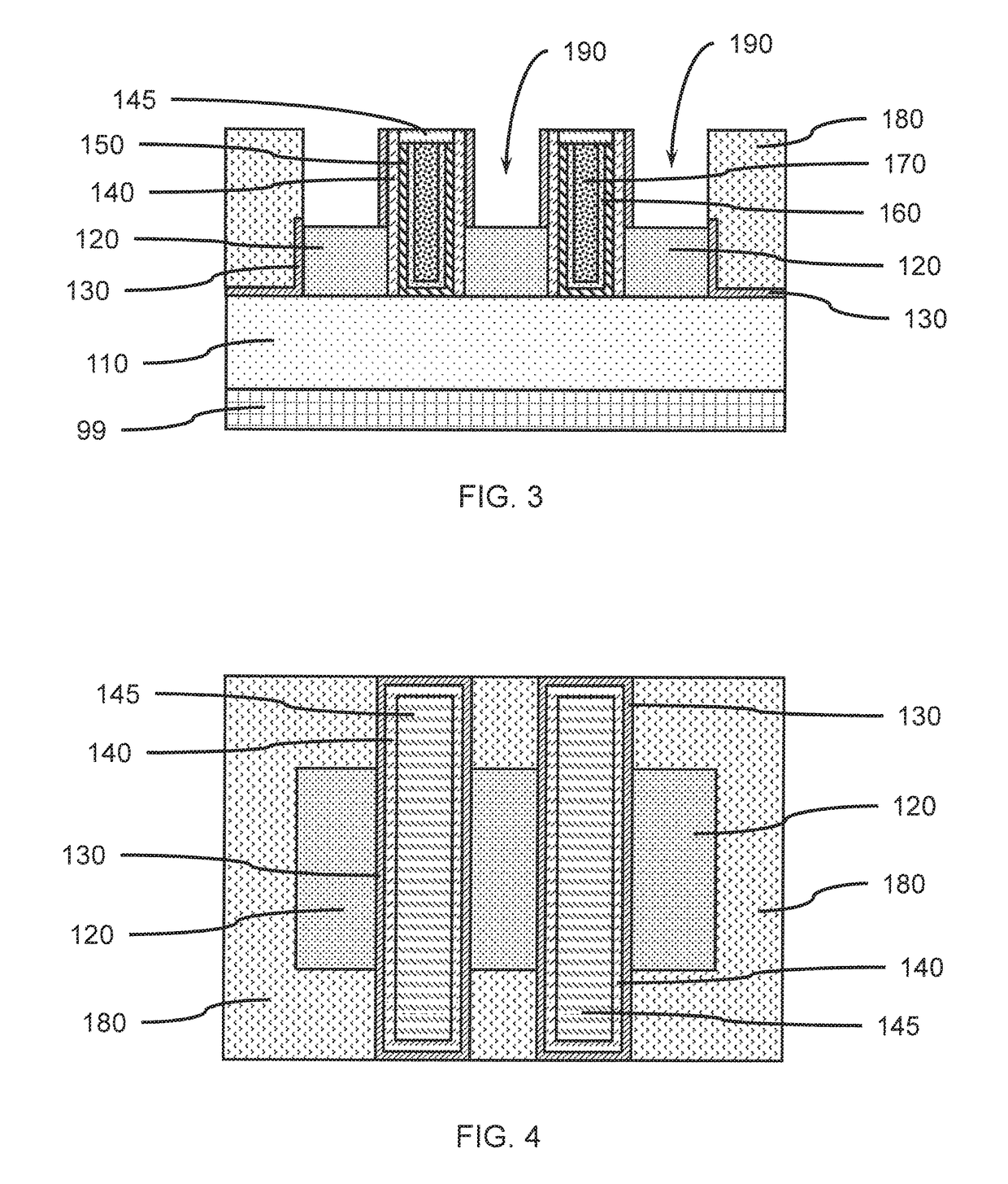
[0034]Principles and embodiments of the present invention relate generally to an approach for reducing the area that a device occupies on a region of a substrate by fabricating gate electrical contacts and source / drain electrical contacts directly above the gate structures and source / drains to eliminate the portions of the source / drains and gate structures that extend outward from the active portions of the device components (e.g., channel, source / drains, metal gate, etc.) for out-of-plane electrical connections, vias, etc.

[0035]Principles and embodiments of the present invention also relate generally to forming self-aligned source / drain and gate contacts to avoid electrical shorting between conductive device features due to misalignment of masking patterns and openings in insulating materials. In particular, self-aligned spacers (e.g., gate sidewall spacers, inner spacers) can be formed on device sidewalls to electrically separate the source / drain terminals from the gate contacts.

[...


PUM


Abstract

A method of forming an active device having self-aligned source/drain contacts and gate contacts, including, forming an active area on a substrate, where the active area includes a device channel; forming two or more gate structures on the device channel; forming a plurality of source/drains on the active area adjacent to the two or more gate structures and device channel; forming a protective layer on the surfaces of the two or more gate structures, plurality of source/drains, and active layer; forming an interlayer dielectric layer on the protective layer; removing a portion of the interlayer dielectric and protective layer to form openings, where each opening exposes a portion of one of the plurality of source/drains; forming a source/drain contact liner in at least one of the plurality of openings; and forming a source/drain contact fill on the source/drain contact liner.

Description

BACKGROUNDTechnical Field[0001]The present invention generally relates to formation of self-aligned gate contacts and source / drain contacts, and more particularly to self-aligned gate contacts and source / drain contacts directly above gate electrodes and source / drains.Description of the Related Art[0002]A Field Effect Transistor (FET) typically has a source, a channel, and a drain, where current flows from the source to the drain, and a gate that controls the flow of current through the channel. Field Effect Transistors (FETs) can have a variety of different structures, for example, FETs have been fabricated with the source, channel, and drain formed in the substrate material itself, where the current flows horizontally (i.e., in the plane of the substrate), and finFETs have been formed with the channel extending outward from the substrate, but where the current also flows horizontally from a source to a drain. The channel for the finFET can be an upright slab of thin rectangular Si,...

Claims


Application Information

Patent Timeline
IPC IPC(8): H01L21/768H01L29/78H01L29/66H01L29/49H01L21/28H01L23/535
CPCH01L29/7851H01L29/66795H01L29/4966H01L23/535H01L21/28088H01L21/76843H01L21/76805H01L21/76897H01L29/41791H01L29/785H01L29/66545H01L21/76883H01L21/76834
Inventor BASKER, VEERARAGHAVAN S.CHENG, KANGGUOSTANDAERT, THEODORUS E.WANG, JUNLI
Owner IBM CORP
Why Eureka
Try Eureka