Level shifter

Active Publication Date: 2018-08-09
ABLIC INC
View PDF0 Cites 0 Cited by
  • Summary
  • Abstract
  • Description
  • Claims
  • Application Information

AI Technical Summary

Benefits of technology

[0010]According to the present invention, when the input-side power supply is stopped or when the rise of the input-side power supply voltage delays at start-up of power supply, the third and fourth MOS transistors and the fifth and sixth MOS transistors serve as a latch circuit, and hence it is possible to maintain the level of the output signal or f

Problems solved by technology

This means that the scale of the

Method used


Image

  • Level shifter
  • Level shifter
  • Level shifter

Examples


first embodiment

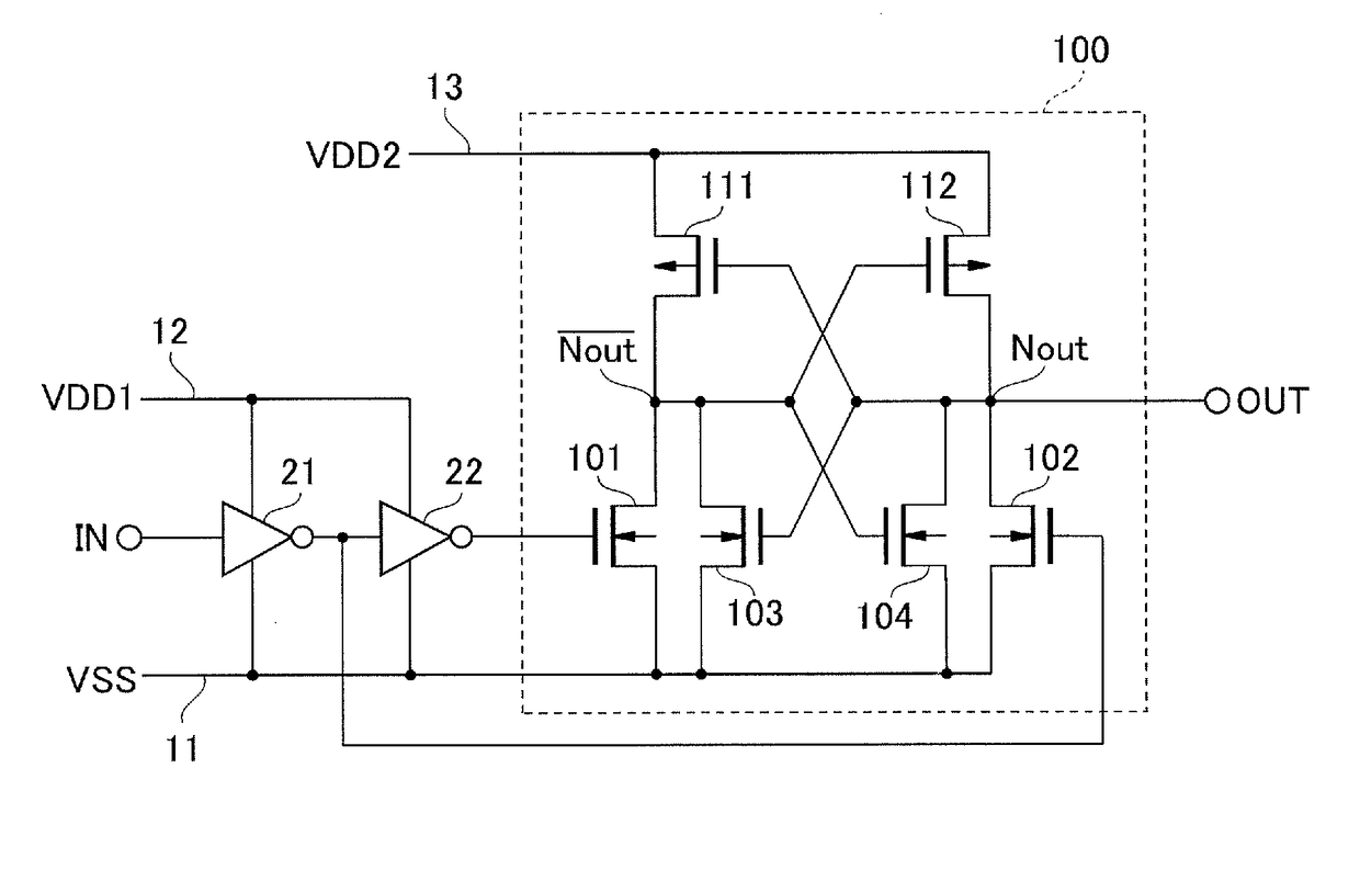
[0017]FIG. 1 is a circuit diagram for illustrating a level shifter 100 according to a first embodiment of the present invention.

[0018]The level shifter 100 is configured to convert an input signal IN having an amplitude between a reference voltage VSS (also referred to as “first power supply voltage”) that is supplied to a power supply line 11 and a power supply voltage VDD1 (also referred to as “second power supply voltage”) that is supplied to a power supply line 12 to a signal having an amplitude between the reference voltage VSS and a power supply voltage VDD2 (also referred to as “third power supply voltage”) that is supplied to a power supply line 13, to thereby output the converted signal as an output signal OUT.

[0019]The level shifter 100 includes NMOS transistors 101, 102, 103, and 104, and PMOS transistors 111 and 112.

[0020]The NMOS transistor 101 is configured to receive a non-inverted signal of the input signal IN at its gate via inverters 21 and 22, and has a source con...

second embodiment

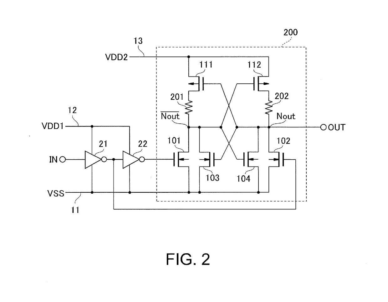
[0045]FIG. 2 is a circuit diagram for illustrating a level shifter 200 according to a second embodiment of the present invention. The same components as those of the level shifter 100 of the first embodiment, which is illustrated in FIG. 1, are denoted by the same reference symbols, and redundant description is omitted as appropriate.

[0046]The level shifter 200 of the second embodiment includes, in addition to the components of the level shifter 100 of the first embodiment, a resistor 201 connected between the PMOS transistor 111 and the inverting output node / Nout, and a resistor 202 connected between the PMOS transistor 112 and the non-inverting output node Nout. The remaining configuration of the level shifter 200 is the same as that of the level shifter 100.

[0047]According to the configuration described above, the same effects as those of the level shifter 100 of the first embodiment are obtained. Specifically, when the input-side power supply is stopped, a level of the output si...

third embodiment

[0049]FIG. 3 is a circuit diagram for illustrating a level shifter 300 according to a third embodiment of the present invention. The same components as those of the level shifter 100 of the first embodiment, which is illustrated in FIG. 1, are denoted by the same reference symbols, and redundant description is omitted as appropriate.

[0050]The level shifter 300 of the third embodiment includes, in addition to the components of the level shifter 100 of the first embodiment, a constant current source 301 connected between the power supply line 13 and the sources of the PMOS transistors 111 and 112. The remaining configuration of the level shifter 300 is the same as that of the level shifter 100.

[0051]Also according to the configuration described above, the same effects as those of the level shifter 100 of the first embodiment are obtained. In addition, due to the provision of the constant current source 301 between the power supply line 13 and the sources of the PMOS transistors 111 an...


PUM


Abstract

Between a power supply potential and a reference potential, a first PMOS transistor and a first NMOS transistor are connected in series via an inverting output node and a second PMOS transistor and a second NMOS transistor are connected in series via a non-inverting output node. A third NMOS transistor is connected in parallel to the first NMOS transistor and a fourth NMOS transistor is connected in parallel to the second NMOS transistor. A gate of the first PMOS transistor and a gate of the third NMOS transistor are connected to the non-inverting output node and a gate of the second PMOS transistor and a gate of the fourth NMOS transistor are connected to the inverting output node. The first and second NMOS transistors receive a non-inverted signal and an inverted signal of an input signal at their gates, respectively.

Description

RELATED APPLICATIONS[0001]This application claims priority under 35 U.S.C. § 119 to Japanese Patent Application No. 2017-022483 filed on Feb. 9, 2017, the entire content of which is hereby incorporated by reference.BACKGROUND OF THE INVENTION1. Field of the Invention[0002]The present invention relates to a level shifter configured to convert an input voltage to a voltage at a different level.2. Description of the Related Art[0003]FIG. 4 is a circuit diagram for illustrating a related-art level shifter 400 (for example, see Japanese Patent Application Laid-open No. 2001-036398).[0004]The related-art level shifter 400 includes NMOS transistors 401 and 402, and PMOS transistors 411 and 412. The level shifter 400 is configured to respectively receive, at gates of the NMOS transistors 401 and 402, a non-inverted signal and an inverted signal of an input signal IN having an amplitude between a reference voltage VSS that is supplied to a power supply line 41 and a power supply voltage VDD1...

Claims


Application Information

Patent Timeline
IPC IPC(8): H03K19/0185
CPCH03K19/018521H03K19/018507H03K3/356104
Inventor SAKAGUCHI, KAORU
Owner ABLIC INC
Why Eureka
Try Eureka