Voltage reference circuit

a voltage reference circuit and voltage reference technology, applied in the direction of electric variable regulation, process and machine control, instruments, etc., can solve the problems of large influence on process variation and temperature characteristics, increase of variability factors due to process variation, disadvantageously increasing circuit scale, etc., to reduce variability in reference voltage level and increase circuit scale

Inactive Publication Date: 2013-03-28
ABLIC INC
View PDF13 Cites 2 Cited by
  • Summary
  • Abstract
  • Description
  • Claims
  • Application Information

AI Technical Summary

Benefits of technology

[0016]With the use of the voltage reference circuit of the present invention, it is possible to reduce variability in a reference voltage level due to process variation by resistance and variability of corrected values of a reference voltage level and temperature characteristics without increasing a circuit scale.

Problems solved by technology

However, in the conventional voltage reference circuit illustrated in FIG. 6, the resistance value as well as the K values and the threshold values of the transistors determine a reference voltage level according to the formula (2), which causes a problem that an influence on process variation and an influence of temperature characteristics are large.
Further, there is also such a problem that variability factors due to process variation increase when correction is performed to reduce a temperature characteristic of the reference voltage level.
Further, in order to perform the correction, it is necessary to include a logic circuit for a temperature sensor and correction, which disadvantageously increases a circuit scale.

Method used


Image

  • Voltage reference circuit
  • Voltage reference circuit
  • Voltage reference circuit

Examples


embodiment 1

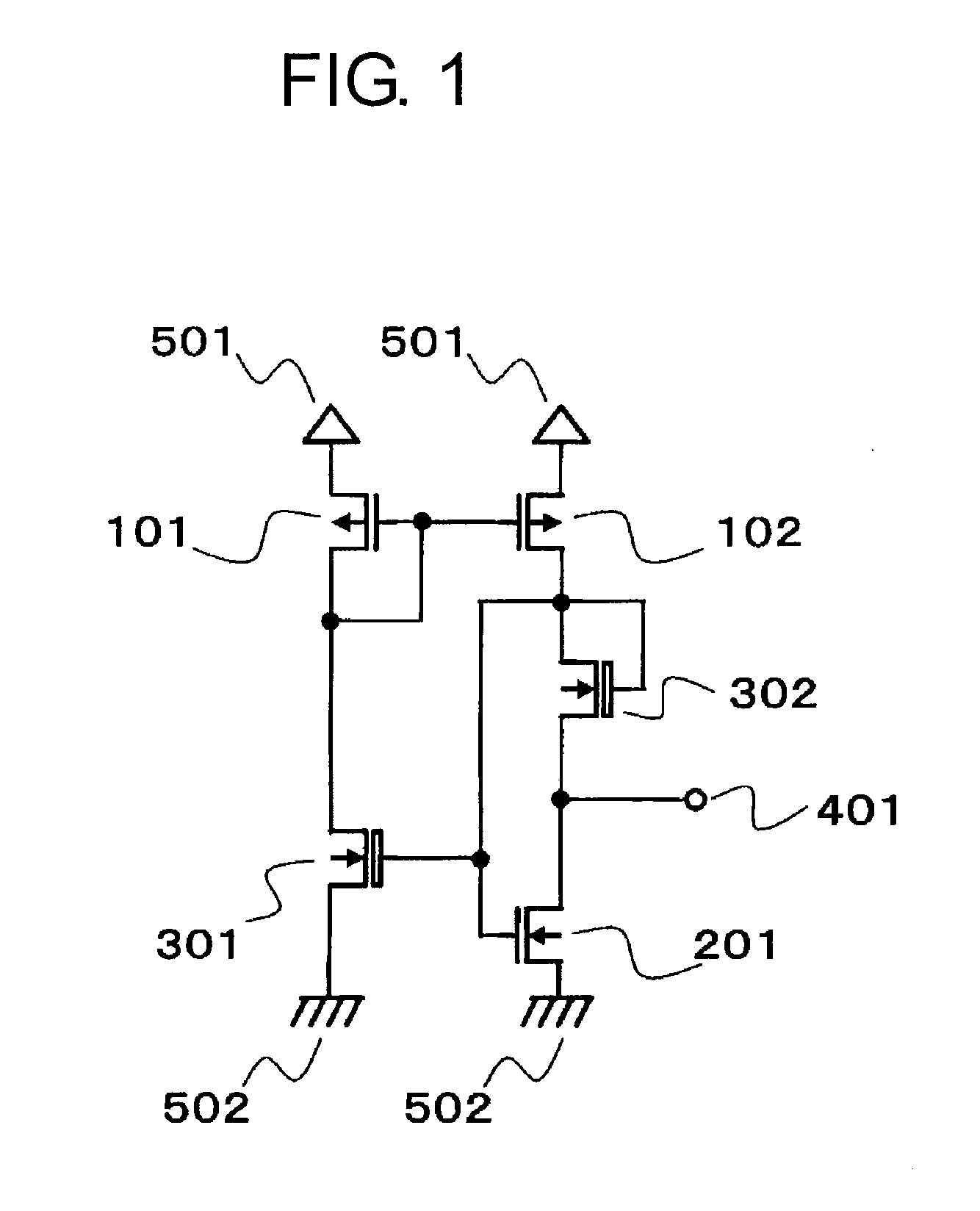
[0024]FIG. 1 is a circuit diagram illustrating a voltage reference circuit according to the first embodiment.

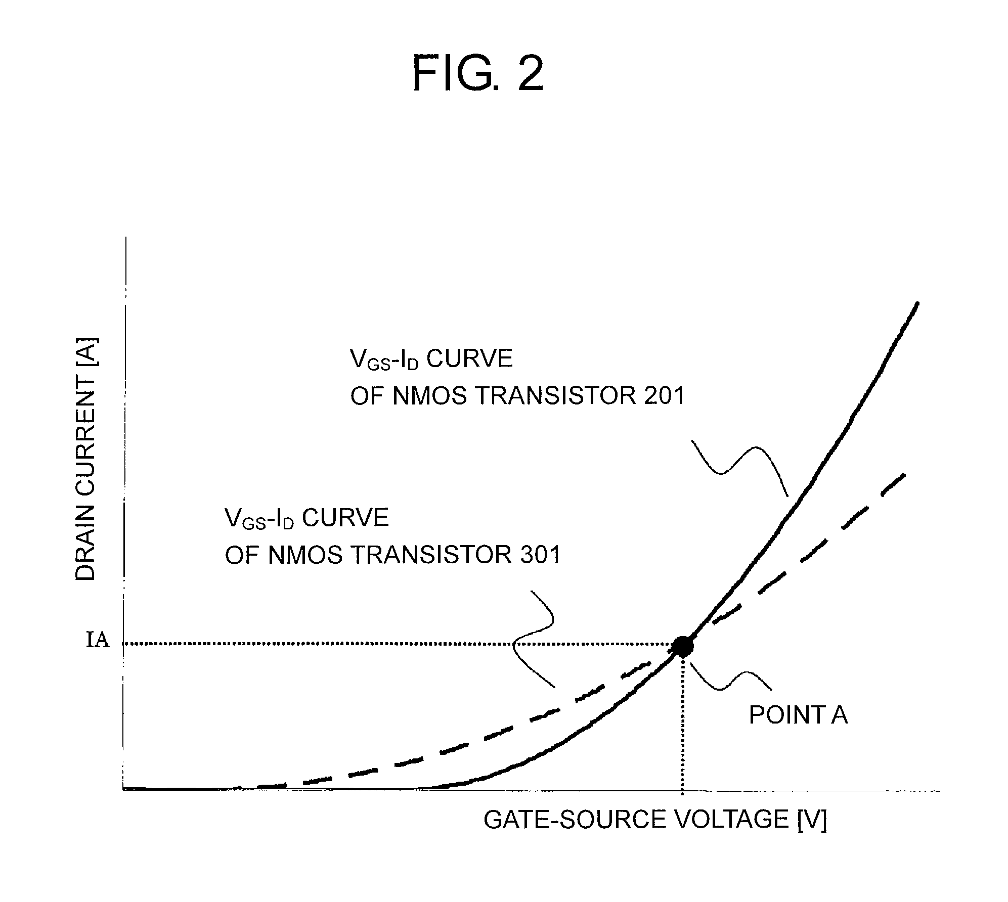
[0025]The voltage reference circuit according to the first embodiment includes PMOS transistors 101 and 102 and NMOS transistors 201, 301, and 302, an output terminal 401, a power supply terminal 501, and an earth terminal 502. A threshold voltage (hereinafter referred to as Vtnl) of the NMOS transistors 301 and 302 is lower than a threshold voltage (hereinafter referred to as Vtnh) of the NMOS transistor 201. Respective K values of the NMOS transistors 201, 301, and 302 are K201 , K301, and K302. The PMOS transistor 101 and the PMOS transistor 102 constitute current mirror circuits.

[0026]Next will be explained connections in the voltage reference circuit according to the first embodiment.

[0027]Source terminals of the PMOS transistors 101 and 102 are connected to the power supply terminal 501. A gate terminal of the PMOS transistors 102 is connected to a gate terminal and a d...

embodiment 2

[0037]FIG. 3 is a circuit diagram illustrating a voltage reference circuit according to the second embodiment.

[0038]The voltage reference circuit according to the second embodiment includes PMOS transistors 101 to 106, NMOS transistors 201 to 204 and 301 to 303, an output terminal 401, a power supply terminal 501, an earth terminal 502, and resistors 601 to 602. A threshold voltage (hereinafter referred to as Vtnl) of the NMOS transistors 301 to 302 is lower than a threshold voltage (hereinafter referred to as Vtnh) of the NMOS transistors 201 to 202. Respective K values of the NMOS transistors 201, 202, 301, and 302 are K201, K202, K301, and K302. Respective resistance values of the resistors 601 and 602 are R601 and R602. The NMOS transistors 203 and 204 constitute a current mirror circuit. The PMOS transistor 101 and the PMOS transistors 102, 103, and 104 constitute current mirror circuits.

[0039]Next will be explained connections of the voltage reference circuit according to the ...

embodiment 3

[0052]FIG. 4 is a circuit diagram illustrating a voltage reference circuit according to the third embodiment.

[0053]The voltage reference circuit according to the third embodiment includes PMOS transistors 101, 701, and 702, NMOS transistors 201 and 202, an output terminal 401, a power supply terminal 501, and an earth terminal 502. An absolute value |Vtpl| of a threshold voltage (hereinafter referred to as Vtpl) of the PMOS transistors 701 and 702 is lower than an absolute value |Vtph| of a threshold voltage (hereinafter referred to as Vtph) of the PMOS transistor 101. Respective K values of the PMOS transistors 101, 701, and 702 are K101, K701, and K702. The NMOS transistors 201 and 202 constitute a current mirror circuit.

[0054]Next will be explained connections of the voltage reference circuit according to the third embodiment. Source terminals of the NMOS transistors 201 and 202 are connected to the earth terminal 502. A gate terminal of the NMOS transistor 202 is connected to a ...


PUM


Abstract

The voltage reference circuit includes: a first MOS transistor; a second MOS transistor including a gate terminal connected to a gate terminal of the first MOS transistor and having an absolute value of a threshold value and a K value higher than an absolute value of a threshold value and a K value of the first MOS transistor; a current mirror circuit flowing a current based on a difference between the absolute values of the threshold values of the first MOS transistor and the second MOS transistor; a third MOS transistor flowing the current; and a fourth MOS transistor having an absolute value of a threshold value and a K value higher than an absolute value of a threshold value of the third MOS transistor and flowing the current.

Description

RELATED APPLICATIONS[0001]This application claims priority under 35 U.S.C. §119 to Japanese Patent Application No. 2011-211220 filed on Sep. 27, 2011, the entire content of which is hereby incorporated by reference.BACKGROUND OF THE INVENTION[0002]1. Field of the Invention[0003]The present invention relates to a voltage reference circuit.[0004]2. Background Art[0005]FIG. 6 is a circuit diagram illustrating a conventional voltage reference circuit.[0006]The conventional voltage reference circuit includes PMOS transistors 101 to 103, NMOS transistors 201 to 204 and 301, an output terminal 401, a power supply terminal 501, an earth terminal 502, and a resistor 601. A threshold voltage (hereinafter referred to as Vtnl) of the NMOS transistor 301 is lower than a threshold voltage (hereinafter referred to as Vtnh) of the NMOS transistors 201 to 204. The PMOS transistors 102 and 103 constitute current mirror circuits with the PMOS transistor 101 to flow a drain terminal current of a desire...

Claims


Application Information

Patent Timeline
Patent Type & Authority Applications(United States)
IPC IPC(8): G05F3/16
CPCG05F3/262G05F3/02G05F3/24G05F3/26
Inventor YAMASAKI, TAROUTSUNOMIYA, FUMIYASU
Owner ABLIC INC
Why Eureka
Try Eureka