Damascene copper wiring image sensor

a damascene copper wiring and image sensor technology, applied in the direction of electrical equipment, semiconductor devices, radio control devices, etc., can solve the problems of compromising the sensitivity of the damascene copper wiring pixel, sin, sic, sicn or like layers used for damascene copper wiring as rie stops, and the cu diffusion barrier is not compatible with optical image sensors, so as to improve the sensitivity of the pixels

Active Publication Date: 2007-03-20
SMARTSENS TECH (HK) CO LTD
View PDF18 Cites 90 Cited by
  • Summary
  • Abstract
  • Description
  • Claims
  • Application Information

AI Technical Summary

Benefits of technology

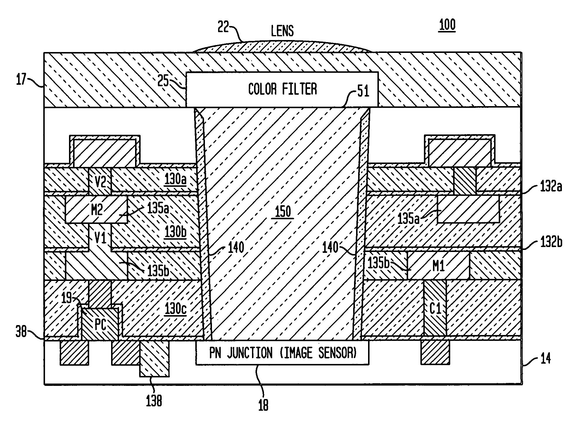
[0010]A number of embodiments of a novel semiconductor optical imager structure that eliminates most or all of the Cu diffusion barrier dielectric material (e.g. a nitride) under the image filtering coatings and lenses. This is accomplished by patterning and etching down to the silicon substrate, either leaving the nitride layer above the image sensor in place or removing it. Alternate embodiments add a dielectric or conductor spacer along the sidewall of the opening, and / or a metal guard ring structure around the opening to eliminate mobile ion contamination issues, and potentially reflect light from the sidewalls to the detector.
[0011]Thus, an image sensor and method of fabrication is provided wherein the image sensor includes Copper (Cu) metallization levels allowing for incorporation of a thinner interlevel dielectric stack with reduced thickness variability to result in a pixel array exhibiting increased light sensitivity. The image sensor is initially fabricated to include thin (e.g. 1–100 nm) dielectric barrier layer (e.g. PECVD or HDPCVD SiN, SiC, SiCN, etc.) above each interlevel Cu metallization that traverses the optical path of each pixel in the sensor array. Then, by implementing a single mask or self-aligned methodologies, an etch is conducted to completely remove the barrier layer metal at locations of the optical path for each pixel in the array, and subsequently, a refill dielectric is provided to fill the etched opening. In alternate embodiments, prior to depositing the refill dielectric, a layer of either reflective or absorptive material is formed along the sidewalls of the etched opening to improve sensitivity of the pixels by either reflecting light to the underlying photodiode or by eliminating light reflections.
[0023]Advantageously, the method for fabricating the image sensor array of pixels includes implementing a single mask or self-aligned mask methodology, that enables a single etch to be conducted to completely remove the dielectric stack and some or all of the barrier layer metals that traverse the optical path for each pixel.
[0024]In alternate embodiments, prior to depositing the refill dielectric, a layer of either reflective or absorptive material may be formed along the sidewalls of the etched opening to improve sensitivity of the pixels by either reflecting light to the underlying photodiode or by eliminating light reflections.

Problems solved by technology

However, none of these state of the art devices described utilize Copper metallization layers in the pixel design.
Thus, the sensitivity of the CMOS imager pixel is compromised.
That is, SiN, SiC, SiCN or like layers used for damascene copper wiring as RIE stop and Cu diffusion barriers are not compatible with optical image sensors due to refractive index mismatch issues.

Method used


Image

  • Damascene copper wiring image sensor
  • Damascene copper wiring image sensor
  • Damascene copper wiring image sensor

Examples


Embodiment Construction

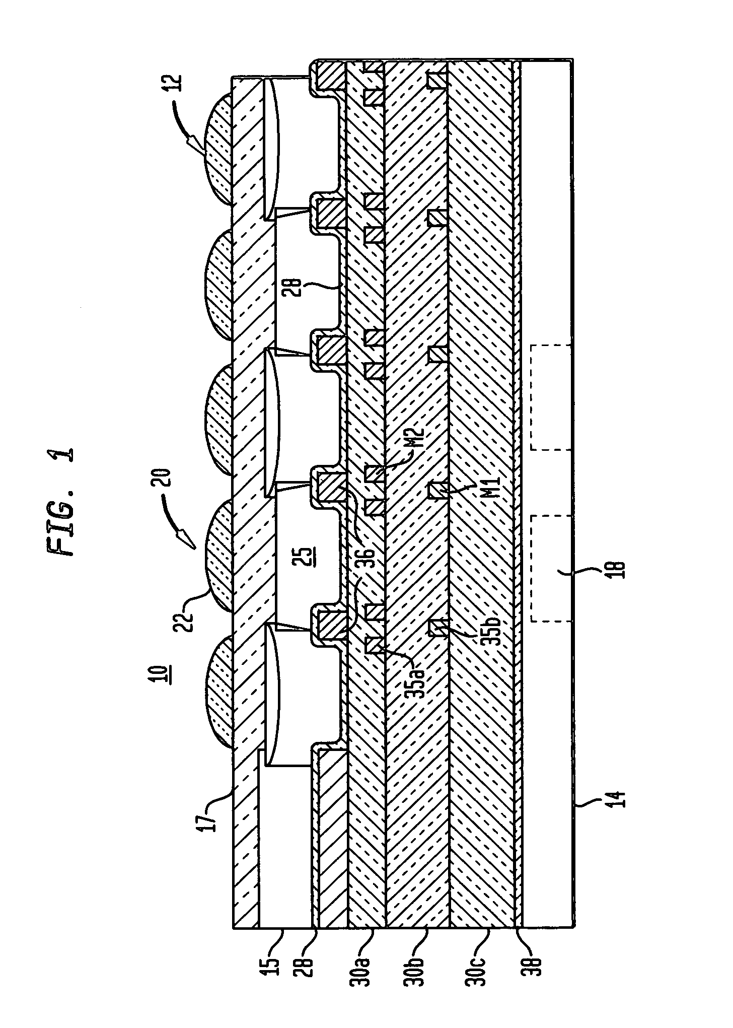
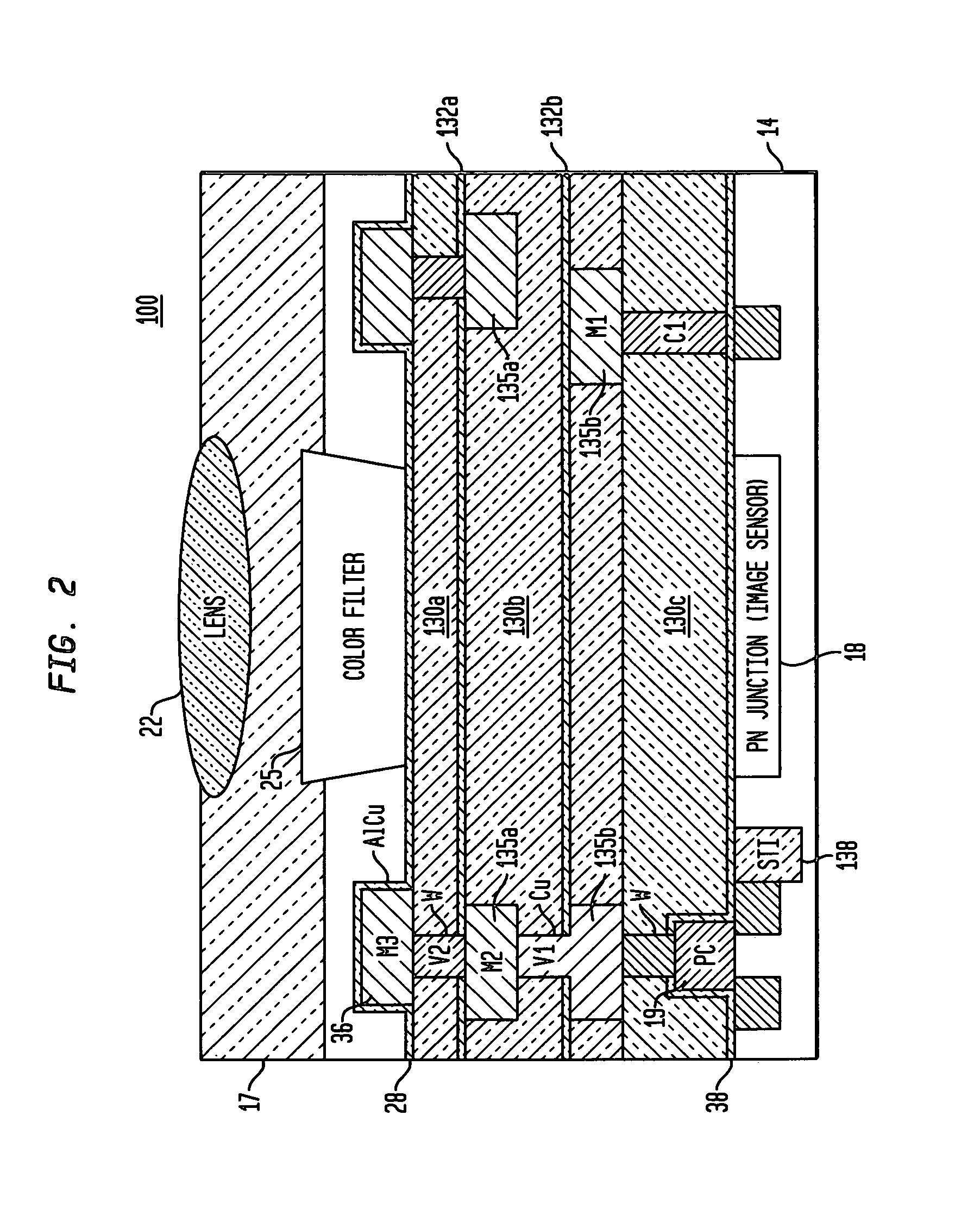
[0038]FIG. 1 depicts image sensor pixel array 10. As shown, the array comprises a plurality of microlenses 12, each having a hemisphere shape, arranged on a smooth planarization layer 17, e.g., a spin on polymer, that is formed on top of a color filter array 15 enabling formation of the microlens array. The color filter array 15 includes individual red, green and blue filter elements 25 (primary color filters) or alternately, cyan, magenta and yellow filter elements (complementary color filter). Each microlens 22 of the microlens array 12 is aligned with a corresponding color filter element 25 and comprises an upper light receiving portion of a pixel 20. The pixel 20 includes a cell portion fabricated upon a semiconductor substrate 14 portion including a stack of comprising one or more interlevel dielectric layers 30a–30c incorporating metallization interconnect levels M1, M2 Aluminum (Al) wire layers 35a, 35b. Interlevel dielectric materials may comprise a polymer or SiO2, for exam...


PUM

PropertyMeasurementUnit
dielectric constantaaaaaaaaaa
thicknessaaaaaaaaaa
thicknessaaaaaaaaaa

Abstract

An image sensor array and method of fabrication wherein the sensor includes Copper (Cu) metallization levels allowing for incorporation of a thinner interlevel dielectric stack with improved thickness uniformity to result in a pixel array exhibiting increased light sensitivity. In the sensor array, each Cu metallization level includes a Cu metal wire structure formed at locations between each array pixel and, a barrier material layer is formed on top each Cu metal wire structure that traverses the pixel optical path. By implementing a single mask or self-aligned mask methodology, a single etch is conducted to completely remove the interlevel dielectric and barrier layers that traverse the optical path. The etched opening is then refilled with dielectric material. Prior to depositing the refill dielectric, a layer of either reflective or absorptive material is formed along the sidewalls of the etched opening to improve sensitivity of the pixels by either reflecting light to the underlying photodiode or by eliminating light reflections.

Description

CROSS REFERENCE TO RELATED APPLICATIONS[0001]The present invention is related to commonly-owned co-pending U.S. patent application Ser. No. 10 / 905,277 filed Dec. 23, 2004 and entitled AN IMAGE SENSOR WITH CU WIRING AND METHOD OF ELIMINATING HIGH REFLECTIVITY INTERFACES THEREFROM, the whole contents and disclosure of which is incorporated by reference as if fully set forth herein.BACKGROUND OF THE INVENTION[0002]1. Field of the Invention[0003]The present invention related generally to the fabrication of semiconductor pixel imager arrays, and more particularly, to a novel semiconductor pixel imager structure and novel process therefor for increasing the sensitivity of the optical image sensors by optimizing the dielectric layer under the lenses.[0004]2. Description of the Prior Art[0005]CMOS image sensors are beginning to replace conventional CCD sensors for applications requiring image pick-up such as digital cameras, cellular phones, PDA (personal digital assistant), personal comput...

Claims


Application Information

Patent Timeline
Patent Type & Authority Patents(United States)
IPC IPC(8): H01L27/14
CPCH01L21/76819H01L21/76834H01L21/76838H01L27/14627H01L27/14685H01L27/14621H01L27/14687H01L27/14636H01L27/146
Inventor ADKISSON, JAMES W.GAMBINO, JEFFREY P.JAFFE, MARK D.LEIDY, ROBERT K.STAMPER, ANTHONY K.
Owner SMARTSENS TECH (HK) CO LTD
Why Eureka
Try Eureka