Thin silicon wafer and method of manufacturing the same

a technology of thin silicon and manufacturing methods, applied in the direction of basic electric elements, electrical apparatus, semiconductor devices, etc., can solve the problems of significantly deteriorating electrical characteristics of devices, significant deterioration of device characteristics, and mixing of impurities such as heavy metals, so as to improve maintain the flexural strength, and reduce the flexural strength of the wafer

Inactive Publication Date: 2009-10-15
SUMCO CORP
View PDF3 Cites 14 Cited by
  • Summary
  • Abstract
  • Description
  • Claims
  • Application Information

AI Technical Summary

Benefits of technology

[0022]In the present invention, a minute damaged layer, serving as a gettering sink, is formed on the rear surface of a thin silicon wafer that is subjected to chemical mechanical polishing using hard abrasive grains having a specific average size distribution. In contrast, in the related art, since the flexural strength of a wafer is lowered due to a damaged layer formed in a polishing process, the damaged layer is removed by chemical mechanical polishing (CMP). In this case, since the damaged layer is removed by CMP, the flexural strength of the wafer is improved. However, there is no gettering sink that prevents the occurrence of heavy metal contamination during the CMP process or the subsequent process thereof. Therefore, when heavy metal contamination occurs in a process after the CMP process, it is likely to have an adverse effect on the electrical characteristics of a device. In contrast, in the present invention, the damaged layer on the rear surface of a wafer is maintained in a range capable of maintaining the flexural strength, and it is possible

Problems solved by technology

When impurities, such as heavy metal, are mixed with the silicon wafer, the device characteristics significantly deteriorate.
However, there is a concern that impurities, such as heavy metal, will be mixed with a silicon wafer for an after process in a semiconductor device process, particularly, a thinning process of polishing the rear surface of the wafer to reduce the thickness of the wafer to about 50 μm.
When impurities, such as heavy metal, are mixed with the silicon wafer, electrical characteristics of a device significantly deteriorate.
In general, during a thinning process, which is an after process in the semiconductor device process, the heat tr

Method used


Image

  • Thin silicon wafer and method of manufacturing the same
  • Thin silicon wafer and method of manufacturing the same
  • Thin silicon wafer and method of manufacturing the same

Examples


Embodiment Construction

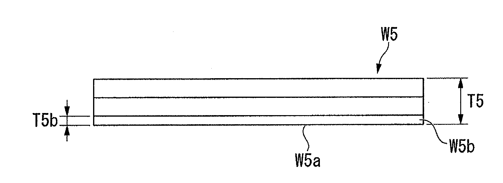
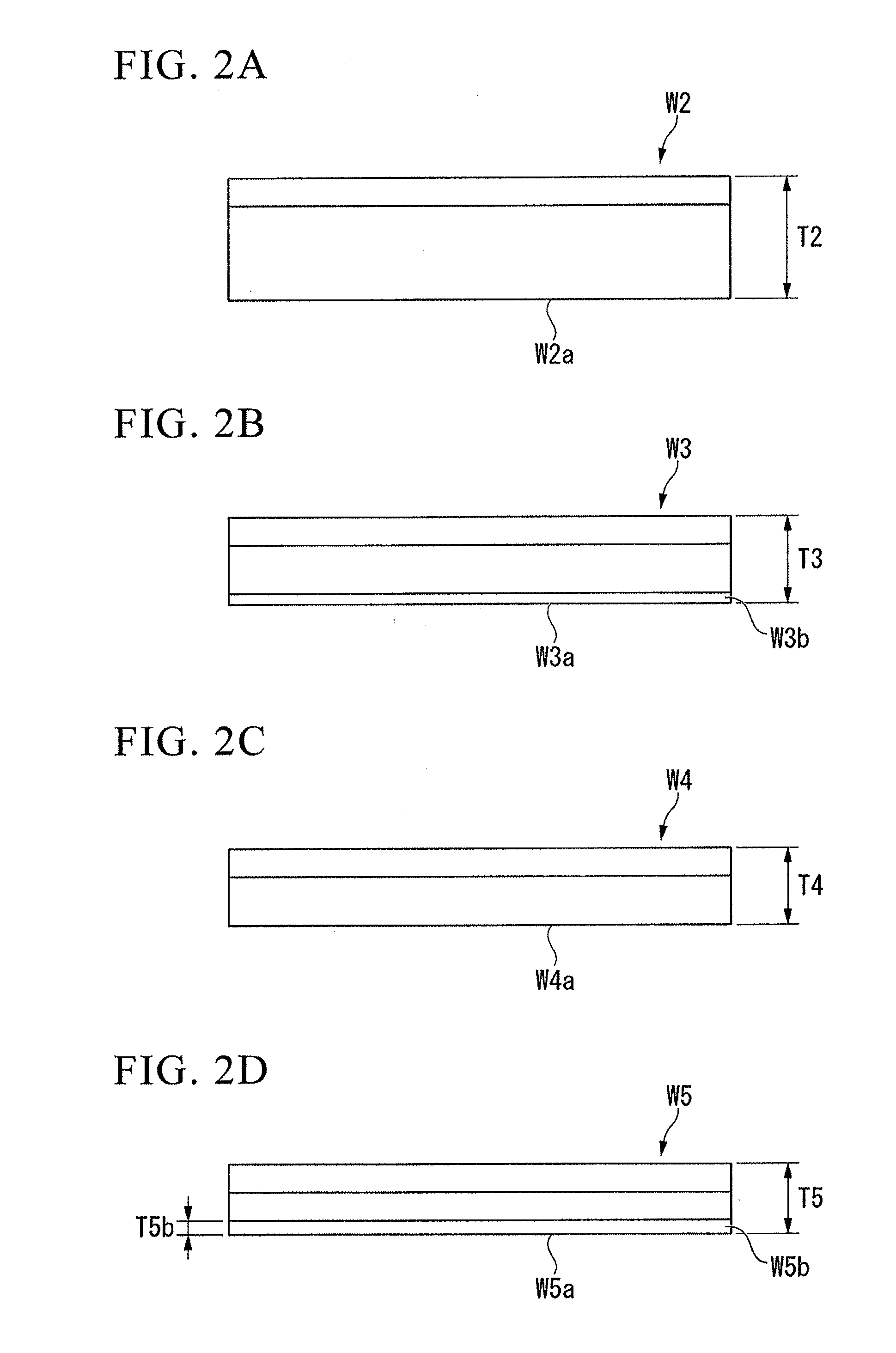
[0030]According to an embodiment of the present invention, there is provided a silicon wafer manufactured from a silicon single crystal that is grown by a CZ method to have a carbon concentration in the range of 1.0×10¹⁶ atoms / cm3 to 1.0×10¹⁷ atoms / cm3 and an initial oxygen concentration in the range of 1.4×10¹⁸ atoms / cm3 to 1.6×10¹⁸ atoms / cm3. A device is formed on the surface of the silicon wafer, and the silicon wafer has a thickness that is greater than or equal to 5 μm and equal to or less than 40 μm.

[0031]In this embodiment, the oxygen concentration is measured by ASTM F121-1979.

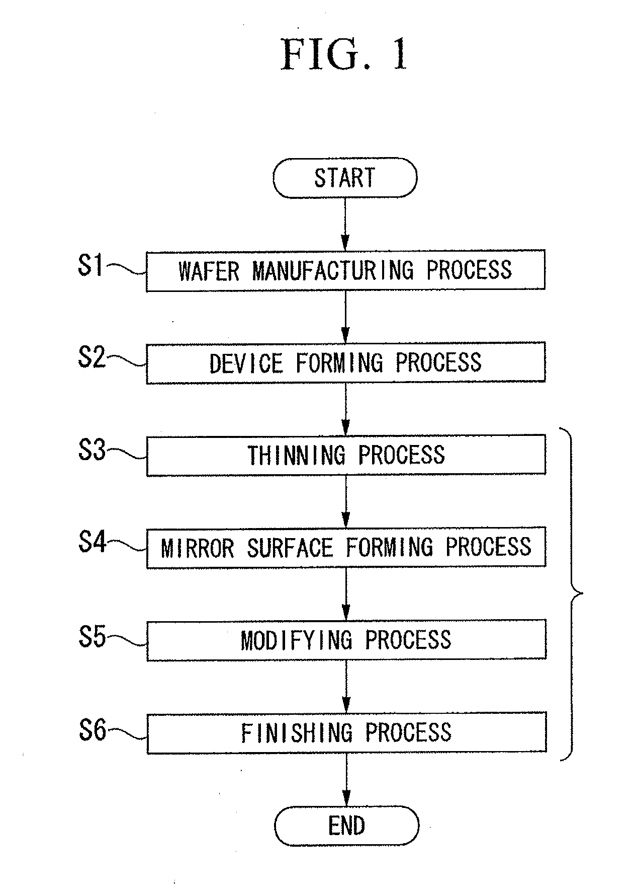
[0032]A modifying process of the present invention may be a polishing process of polishing the surface of the silicon wafer and a CMP process using hard slurry that is made of colloidal silica, silicon crystal, or diamond-like carbon and has a hardness in the range of 200 HV to 1000 HV.

[0033]The device formed on the silicon wafer according to the present invention may be a memory device.

[0034]Hereinaft...


PUM


Abstract

A method of manufacturing a thin silicon wafer by slicing a silicon single crystal includes: a thinning step S3 of polishing a rear surface of the silicon wafer to reduce the thickness of the silicon wafer after a device structure is formed on a front surface of the silicon wafer; a mirror surface forming step S4 of processing the rear surface of the silicon wafer into a mirror surface using a chemical mechanical polishing method; and a modifying step S5 of dispersing abrasive grains that are harder than those used to form the mirror surface in the mirror surface forming process and forming a damaged layer, serving as a gettering sink for heavy metal, on the rear surface of the silicon wafer using the chemical mechanical polishing method. The thickness T5b of the damaged layer W5b in a wafer depth direction is set by the chemical mechanical polishing method in the modifying step S5 to control the gettering capability of the damaged layer.

Description

BACKGROUND OF THE INVENTION[0001]1. Field of the Invention[0002]The present invention relates to a thin silicon wafer and a method of manufacturing the same, and more particularly, to a technique for polishing the rear surface of a silicon wafer, which is formed by a before process in a semiconductor device process, using a chemical mechanical polishing method for an after process in the semiconductor device process to give gettering capability to the thin silicon wafer.[0003]Priority is claimed on Japanese Patent Application No. 2008-105781, filed Apr. 15, 2008, the content of which is incorporated herein by reference.[0004]2. Description of Related Art[0005]With the development of mobile phone and digital still camera techniques, the thickness of a semiconductor device package provided in the apparatus has been reduced.[0006]Such a thin semiconductor device is manufactured by slicing a silicon single crystal pulled by, for example, a CZ (Czochralski) method into a silicon wafer an...

Claims


Application Information

Patent Timeline
IPC IPC(8): H01L29/34H01L21/304H01L21/322
CPCH01L21/30625H01L29/34H01L21/3221
Inventor KURITA, KAZUNARIOMOTE, SHUICHI
Owner SUMCO CORP
Why Eureka
Try Eureka