
Cleaning method, method for fabricating semiconductor device and cleaning solution

a cleaning method and semiconductor technology, applied in the field of cleaning techniques, can solve the problems of affecting the cleaning effect, and affecting the cleaning effect, and achieve the effect of efficient removal of metal contamination

Inactive Publication Date: 2006-02-14
RENESAS ELECTRONICS CORP
View PDF9 Cites 14 Cited by
  • Summary
  • Abstract
  • Description
  • Claims
  • Application Information

AI Technical Summary

Benefits of technology

[0014]An object of the present invention is to provide a cleaning technique for efficiently removing metal contamination adhered onto a surface of a substrate without damaging an underlayer.
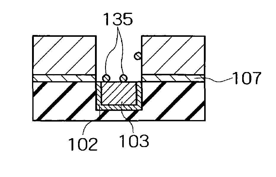
[0015]Another object of the present invention is to provide a cleaning technique for allowing efficient removal of metal contamination adhered onto surfaces of a copper wiring and an insulating film without generating slits at the boundary between the copper wiring and a barrier metal film and damaging the surface of the copper wiring in a copper wiring formation process.
[0016]A further object of the present invention is to provide a technique allowing the removal of a mask or a contaminant without damaging the underlayer in a mask stripping process.

Problems solved by technology

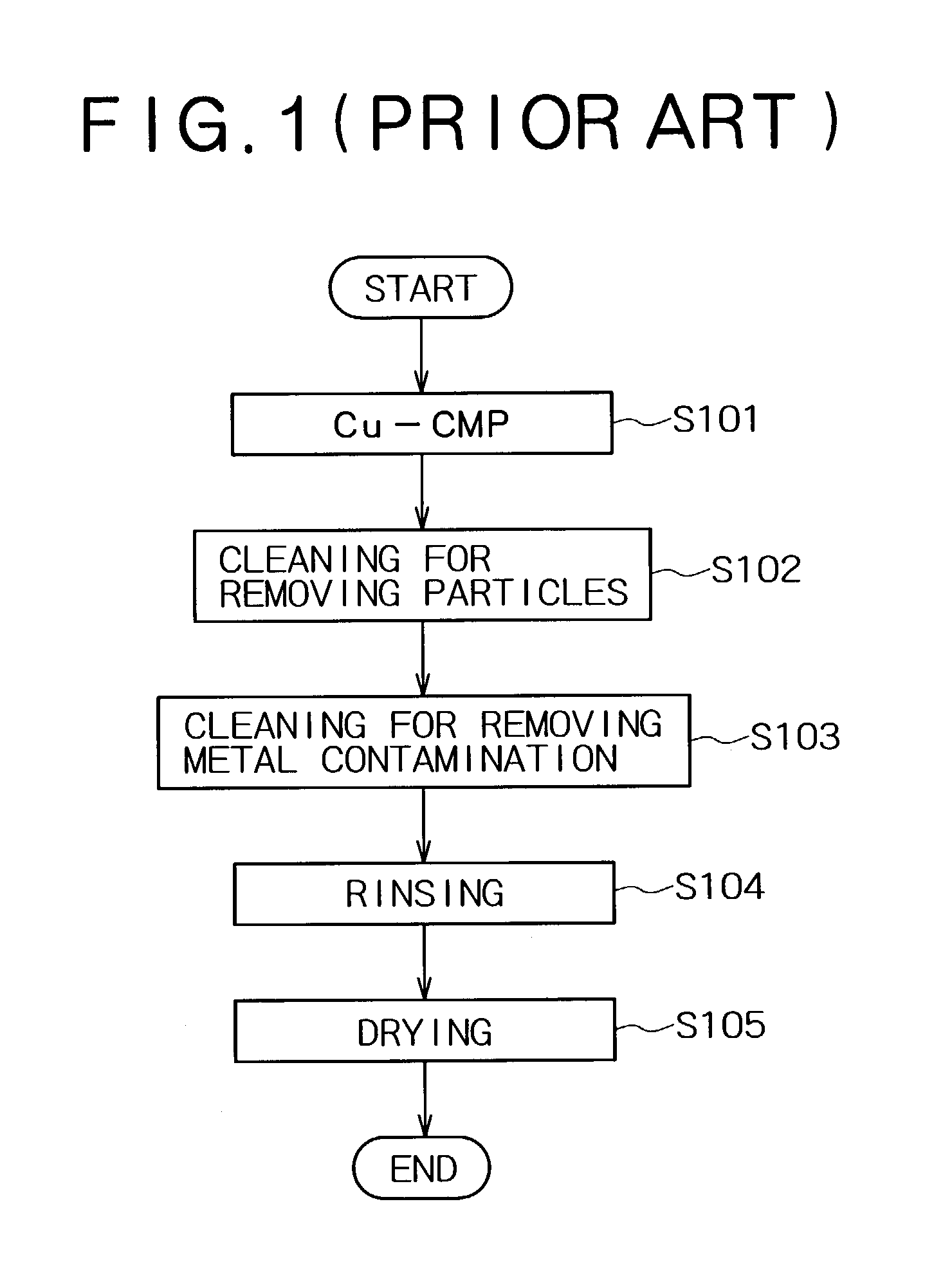
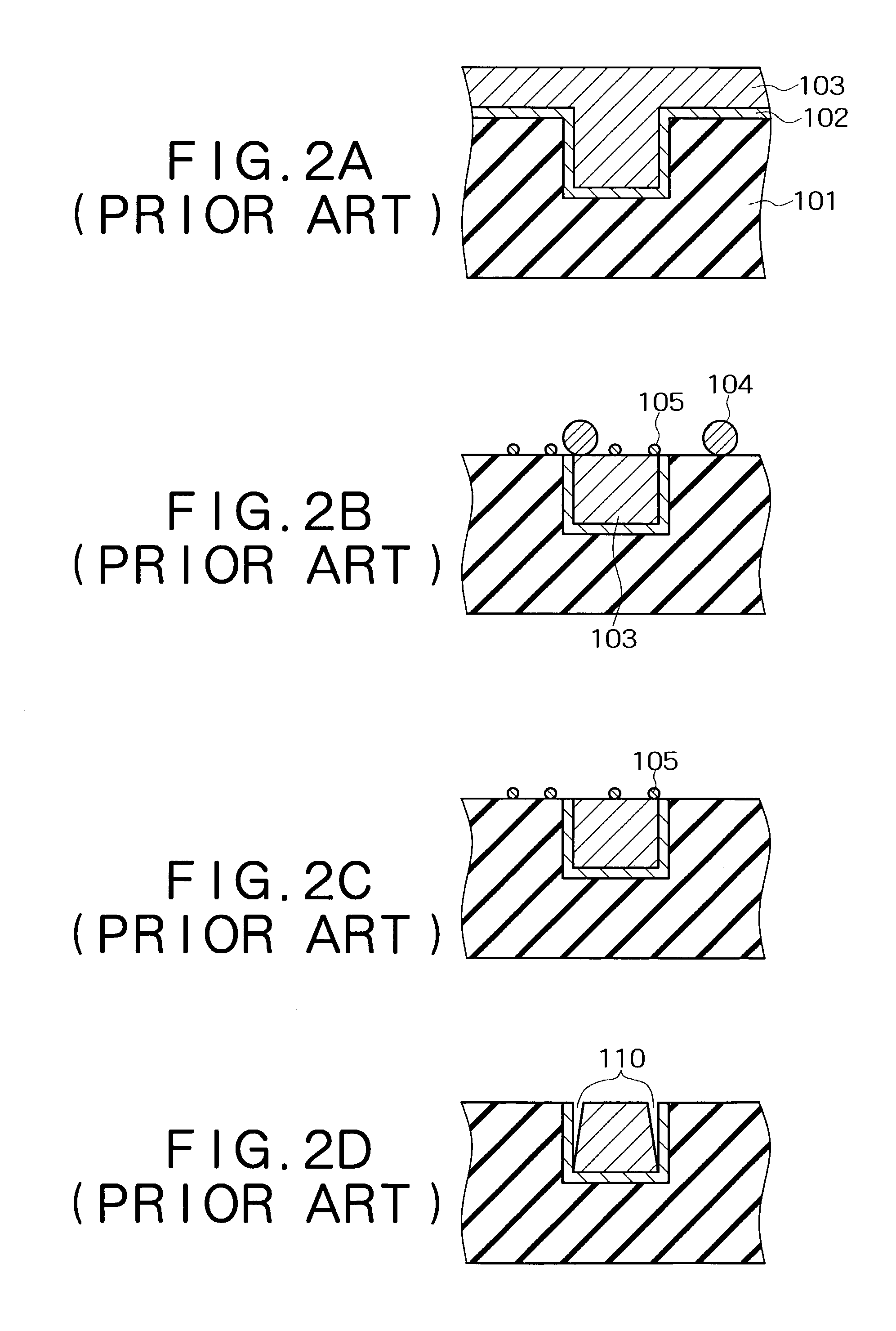
However, since the CMP is a process for polishing a copper film with polishing particles, a large amount of particles or metal contamination are adhered to a surface of a wafer as the result of CMP.
In the case where such slits are generated, there arises a problem in that the degradation in reliability (resistance against electromigration or the like) of the copper wiring is induced.
In addition, when a film is to be formed in the wiring layer, the flatness of the film is lost.
It is difficult to completely prevent the generation of such slits even if an anticorrosive is added to an organic acid cleaning solution.
In each of the above-described processes, not only the generation of the slits, but also an increase in resistance due to increased roughness of the surface of the copper film and a drop in resistance against electromigration become problems in some cases.
These problems arise because an oxide film present on the surface of the copper film is dissolved in acid to generate minute concave and convex portions on the surface of the copper film.
As a result, a desired hole shape cannot be obtained in some cases.
As described above, if acid cleaning for removing the metal contamination is conducted in the semiconductor device fabrication process, there arise various problems such as the generation of slits in the metal film or the damages to the underlayer.
However, although these cleaning solutions are effective for removing the metal contamination of specific metals such as iron metals, it is difficult to remove metal contamination of hardly removable metals such as copper, or particles containing the same metal as the metal film on which the particles are adhered.
Moreover, in the method of bubbling and dissolving hydrogen in a carbon dioxide aqueous solution, a sufficient amount of hydrogen is not dissolved, so that the oxidation-reduction potential becomes relatively high.
As a result, this method is not necessarily effective to deal with the problems such as the generation of slits or the surface roughness in a copper wiring formation process.

Method used


Image

  • Cleaning method, method for fabricating semiconductor device and cleaning solution
  • Cleaning method, method for fabricating semiconductor device and cleaning solution
  • Cleaning method, method for fabricating semiconductor device and cleaning solution

Examples


example 1

[0106]The process described with reference to FIGS. 9A to 9D was actually implemented so as to measure the cleaning performance of cleaning solutions. As cleaning solutions, the following four cleaning solutions were prepared to confirm the cleaning performance of each of the cleaning solutions.[0107]Cleaning solution 1: an aqueous solution of oxalic acid at 0.1 percent by mass;[0108]Cleaning solution 2: an aqueous solution of oxalic acid at 0.1 percent by mass in which 1 ppm of a hydrogen gas is dissolved;[0109]Cleaning solution 3: an aqueous solution containing oxalic acid at 0.1 percent by mass and EDTA at 0.1 percent by mass in which 1 ppm of a hydrogen gas is dissolved; and[0110]Cleaning solution 4: an aqueous solution of HCl at pH 5.

[0111]An oxidation-reduction potential of the cleaning solution 1 was about 380 mV, and that of the cleaning solution 2 was about −200 mV. The cleaning solution 1 had a pH value of about 2.0, and the cleaning solution 2 had a pH value of about 2.2....

example 2

[0119]After formation of the copper film on the silicon substrate, a cleaning treatment was conducted with predetermined cleaning solutions. Thereafter, the roughness on the surface of the copper film was measured.

[0120]As cleaning solutions, the following three cleaning solutions were used.[0121](a) oxalic acid (0.03 percent by mass);[0122](b) oxalic acid (0.03 percent by mass)+hydrogen (1 ppm); and[0123](c) oxalic acid (0.03 percent by mass)+a reducing agent (0.1 percent by mass).

where the reducing agent is sodium dithionite.

[0124]The oxidation-reduction potential of the cleaning solution (a) was about 380 mV, the oxidation-reduction potential of the cleaning solution (b) was about −200 mV, and the oxidation-reduction potential of the cleaning solution (c) was about 50 mV. The measurement of the oxidation-reduction potential was implemented under the same conditions as those in Example 1. The cleaning solution (a) had a pH value of about 2.5, the cleaning solution (b) had a pH val...


PUM


Abstract

A cleaning solution having an oxidation-reduction potential lower than that of pure water and a pH value of 4 or below is used to remove metal contamination, thereby efficiently removing the metal contamination adhered onto a surface of a substrate without damaging an underlayer.

Description

BACKGROUND OF THE INVENTION[0001]1. Field of the Invention[0002]The present invention relates to a cleaning technique employed in a process of fabricating a semiconductor device, in particular, to a substrate cleaning technique for cleaning a substrate having a surface on which a metal material is exposed.[0003]2. Description of the Related Art[0004]Recently, in view of a higher operation speed of logic devices, a copper wiring having low resistance, excellent in resistance against electromigration, has been widely used. Since the copper is hard to process by dry etching, a wiring pattern is formed by a Damascene process utilizing CMP (Chemical Mechanical Polishing) in the case where a copper wiring is to be formed. However, since the CMP is a process for polishing a copper film with polishing particles, a large amount of particles or metal contamination are adhered to a surface of a wafer as the result of CMP. Therefore, it is important to thoroughly clean the surface of the wafer ...

Claims


Application Information

Patent Timeline
IPC IPC(8): H01L21/302G03F7/40C11D7/02C11D7/26C11D7/32C11D11/00C11D17/08G03F7/42H01L21/02H01L21/027H01L21/304H01L21/311H01L21/321H01L21/768
CPCC11D7/265C11D7/3245H01L21/02074G03F7/422H01L21/02063C11D11/0047C11D2111/22
Inventor AOKI, HIDEMITSUTOMIMORI, HIROAKIYAMAMOTO, KENICHI
Owner RENESAS ELECTRONICS CORP
Learn More