Array Substrate And Liquid Crystal Display Panel

a liquid crystal display and substrate technology, applied in static indicating devices, instruments, non-linear optics, etc., can solve the problems of poor image display, deficient display qualities, inadequacies, etc., and achieve the effect of improving the display effect of the lcd, poor image display, and poor charging ability of pixels

Active Publication Date: 2018-12-13
SHENZHEN CHINA STAR OPTOELECTRONICS SEMICON DISPLAY TECH CO LTD
View PDF0 Cites 3 Cited by
  • Summary
  • Abstract
  • Description
  • Claims
  • Application Information

AI Technical Summary

Benefits of technology

[0005]An object of the present disclosure is to propose an array substrate which can compensate a pixel under charging for brightness. A conventional tri-gate driver structure is poor for pixel charging ability, resulting in a pixel with a specific color under charging and further poorer display. The array substrate proposed by the present disclosure can be substituted for the conventional tri-gate driver structure.
[0020]The display effect of the LCD obviously improves by changing the arrangement of subpixels, color mixture of subpixels to compensate pixels under charging for brightness in the present disclosure. In other words, the technical problems of the conventional tri-gate driver structure, such as poor image display and display quality, are resolved due to poor charging ability of pixels which are inclined to incomplete charging. This is the beneficial effect of the present disclosure.

Problems solved by technology

In other words, the pixel charging ability is substandard, which easily causes inadequate charging, bad image display, and deficient display qualities.
A conventional tri-gate driver structure is poor for pixel charging ability, resulting in a pixel with a specific color under charging and further poorer display.
In other words, the technical problems of the conventional tri-gate driver structure, such as poor image display and display quality, are resolved due to poor charging ability of pixels which are inclined to incomplete charging.

Method used


Image

  • Array Substrate And Liquid Crystal Display Panel
  • Array Substrate And Liquid Crystal Display Panel
  • Array Substrate And Liquid Crystal Display Panel

Examples


embodiment 1

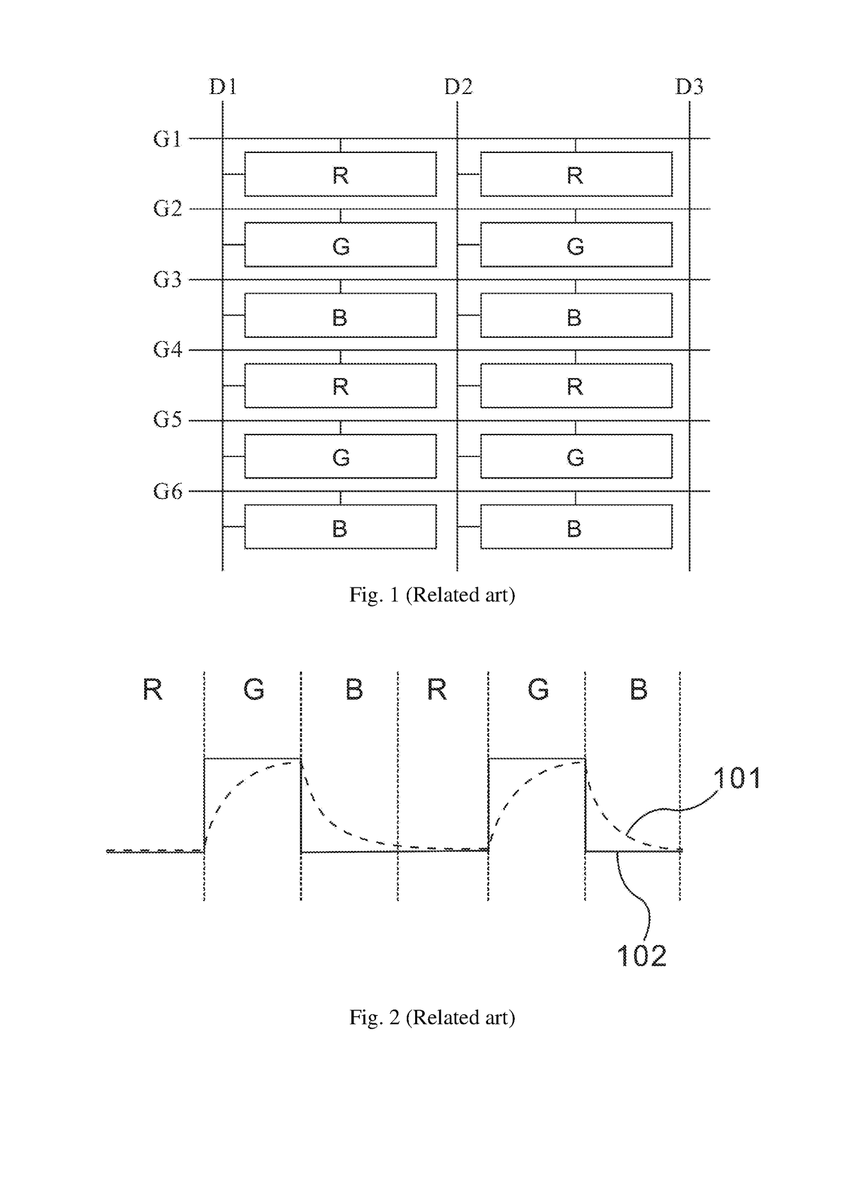
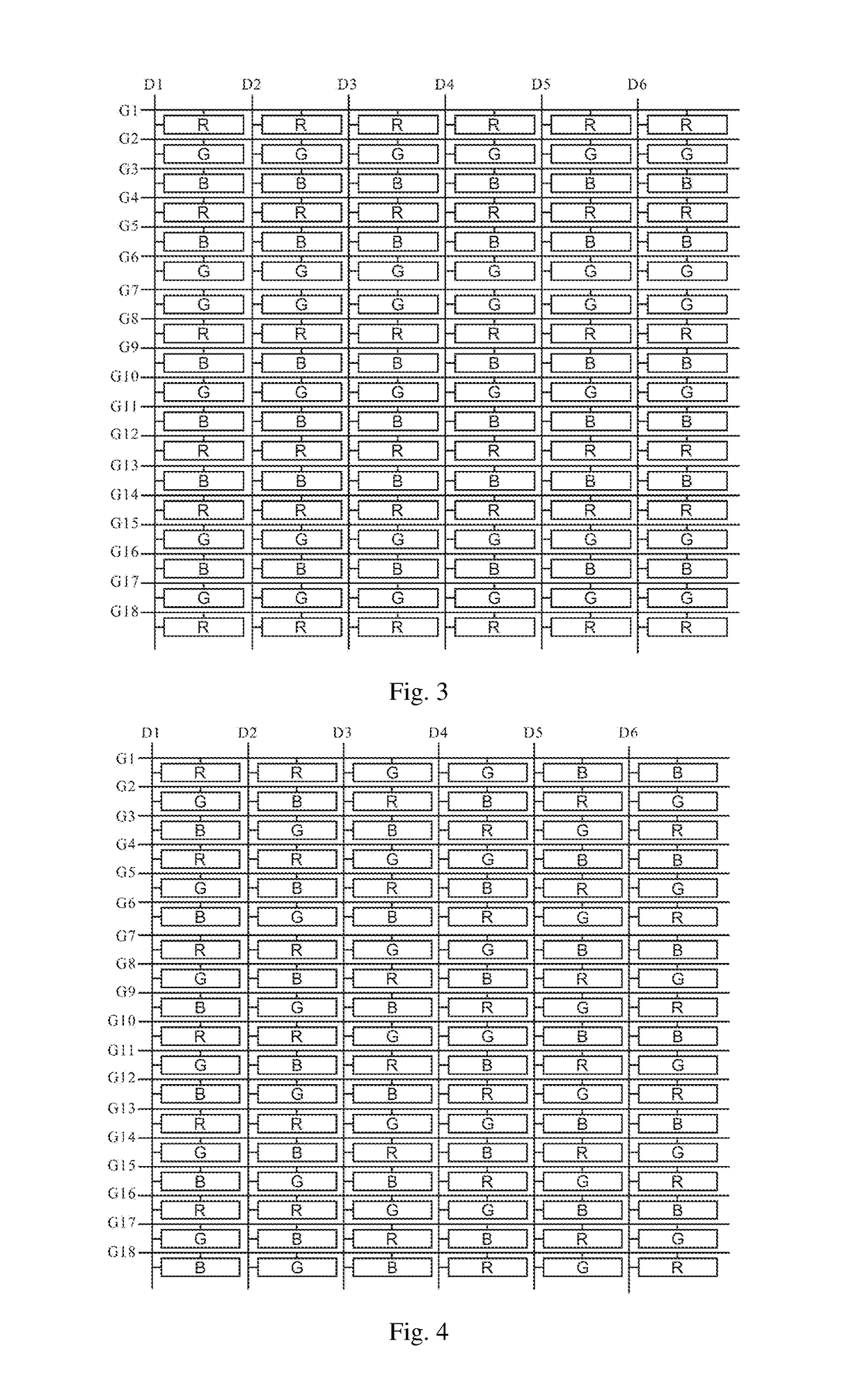
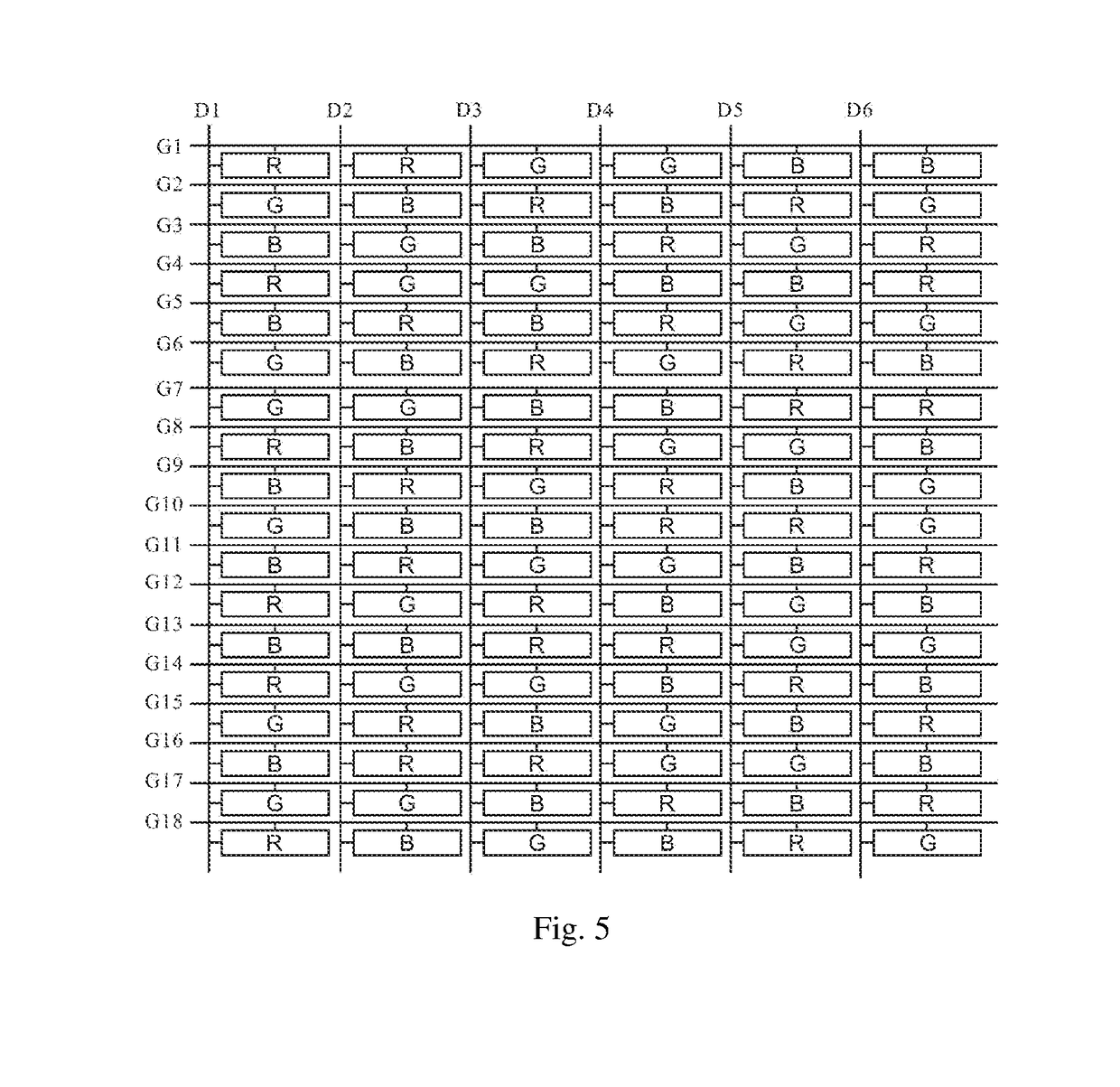
[0032]Please refer to FIG. 3 illustrating a schematic diagram of a pixel of array substrate according to one preferred embodiment of the present disclosure. The array substrate includes a plurality of pixel units arranged in an array. Each of the plurality of pixel units includes a red subpixel R, a green subpixel G, and a blue subpixel B. Each column corresponds to a data line. Each row corresponds to a gate line. Six pixel units arranged horizontally and / or longitudinally are repeatedly arranged in circulation in the pixel structure.

[0033]The subpixels in each of the six consecutive pixel units arranged longitudinally are arranged in a way of RGB, RBG, GRB, GBR, BRG, and BGR successively. Likewise, the subpixels in each of the six consecutive pixel units are arranged horizontally.

[0034]Compared the green subpixel G with the red subpixel R and the blue subpixel B, some of the subpixels are not fully charged when a pure green image is shown. Some of the subpixels and the green subpi...


PUM

PropertyMeasurementUnit
electric fieldaaaaaaaaaa
widthaaaaaaaaaa
timeaaaaaaaaaa

Abstract

An array substrate includes a plurality of display pixels arranged in an array. Each of the plurality of display pixels comprises a red subpixel R, a green subpixel G, and a blue subpixel B. Six of the consecutive display pixels arranged horizontally and / or longitudinally as a whole are repeatedly arranged in a pixel unit. An arrangement order of the subpixels in each of the six consecutive display pixels is totally different. The subpixels in the six consecutive display pixels are arranged as RGB, RBG, GRB, GBR, BRG, and BGR successively. The technical problems of the conventional tri-gate driver structure, such as poor image display and display quality, are resolved due to poor charging ability of pixels which are inclined to incomplete charging.

Description

BACKGROUND1. Field of the Disclosure[0001]The present disclosure relates to the technical field of liquid crystal display, and more particularly, to an array substrate and a liquid crystal display (LCD) including the array substrate.2. Description of the Related Art[0002]A liquid crystal display (LCD) is by far one of the most widely used flat display. The LCD, as a display including a color screen with a high resolution, has been widely applied to a variety of electronic devices such as mobile phones, personal digital assistants (PDAs), digital cameras, computer screens, and laptop screens. used monitor with a high resolution color screen. A conventional, widely applied liquid crystal display is formed by upper and lower substrates and a medial liquid crystal layer. The substrates are formed by glass and an electrode, etc. When the upper and lower substrates in the display include an electrode, the display is at a longitudinal electric field mode such as a twist nematic (TN) mode, ...

Claims


Application Information

Patent Timeline
Patent Type & Authority Applications(United States)
IPC IPC(8): G02F1/1362G02F1/1335
CPCG02F1/136286G02F1/133514G02F2201/52G09G3/3607G09G2320/0242G02F1/1362G02F1/136222G09G2300/0452
Inventor HAO, SIKUN
Owner SHENZHEN CHINA STAR OPTOELECTRONICS SEMICON DISPLAY TECH CO LTD
Why Eureka
Try Eureka