
Display panel and display device

Active Publication Date: 2019-02-07
XIAMEN TIANMA MICRO ELECTRONICS
View PDF0 Cites 0 Cited by
  • Summary
  • Abstract
  • Description
  • Claims
  • Application Information

AI Technical Summary

Benefits of technology

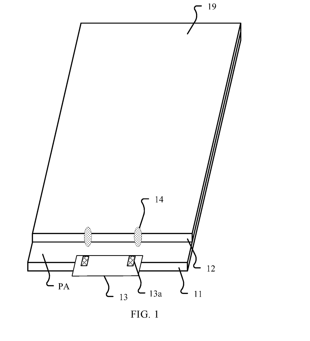
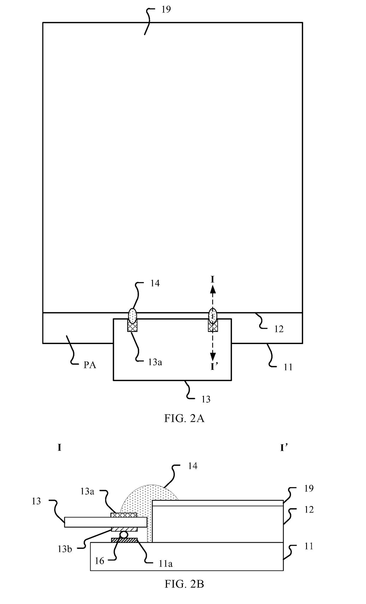
This patent describes a display panel that includes a first substrate with a step area and a second substrate opposite to the first substrate. The second substrate has a first surface facing the first substrate and an opposite second surface. A Chip On Flex (COF) is disposed on the step area of the first substrate and includes at least one ground pad. The COF has a first surface facing the first substrate, a second surface opposing the first surface, and a first side intersecting with the first surface and the second surface, respectively. A conductive layer is disposed on the second surface of the second substrate, and a conductive adhesive is electrically connected to the conductive layer and at least the first component of the at least one ground pad. The technical effect of this patent text is to provide an improved display panel that efficiently connects to the substrate and increases the overall display panel's reliability and stability.

Problems solved by technology

However, as the display technology advances, the resolution of the display panel is getting higher and higher, more wires (such as data wires for transmitting data signals) are going to be disposed in the frame / border area (especially the lower frame area) of the display panel, and the ground pad also occupies a part of the lower frame area, which in turn enlarges the lower frame area (also called a step area) and is not favorable for narrowing the frame of the display panel.

Method used


Image

  • Display panel and display device
  • Display panel and display device
  • Display panel and display device

Examples


Embodiment Construction

[0031]Reference will now be made in detail to exemplary embodiments of the disclosure, which are illustrated in the accompanying drawings. Hereinafter, embodiments consistent with the disclosure will be described with reference to drawings. In the drawings, the shape and size may be exaggerated, distorted, or simplified for clarity. Wherever possible, the same reference numbers will be used throughout the drawings to refer to the same or like parts, and a detailed description thereof may be omitted.

[0032]Further, in the present disclosure, the disclosed embodiments and the features of the disclosed embodiments may be combined under conditions without conflicts. It is apparent that the described embodiments are some but not all of the embodiments of the present disclosure. Based on the disclosed embodiments, persons of ordinary skill in the art may derive other embodiments consistent with the present disclosure, all of which are within the scope of the present disclosure.

[0033]The pr...


PUM


Abstract

A display panel and a display device are provided. The display panel includes a first substrate having a step area; a second substrate disposed opposite to the first substrate, wherein the second substrate has a first surface facing the first substrate and an opposite second surface; a Chip On Flex (COF) disposed on the step area of the first substrate and including at least one ground pad; a conductive layer disposed on the second surface of the second substrate; and a conductive adhesive electrically connected to the conductive layer and the at least one ground pad.

Description

CROSS-REFERENCES TO RELATED APPLICATIONS[0001]This application is a continuation in part of U.S. patent application Ser. No. 15 / 823,133, filed on Nov. 27, 2017, which claims the priority of Chinese Patent Application No. 201710647291.7, filed on Aug. 1, 2017, the entire contents of all of which are incorporated herein by reference.FIELD OF THE DISCLOSURE[0002]The present disclosure generally relates to the display technology and, more particularly, relates to a display panel and a display device.BACKGROUND[0003]Liquid crystal displays (LCDs) are featured with various advantages, such as low radiation, compactness and low energy consumption, which have gradually replaced traditional cathode ray tube (CRT) displays and have been widely used in flat-panel TVs, laptops, and other portable products.[0004]An existing LCD panel often includes an array substrate, a color film substrate, and a liquid crystal layer disposed between the array substrate and the color film substrate. Because sta...

Claims


Application Information

Patent Timeline
IPC IPC(8): G02F1/1345G02F1/1335G02F1/1362
CPCG02F1/13452G02F1/133528G02F1/136286G02F1/136204G02F2202/28G02F2202/16H01L27/3244G02F1/13458G02F2202/22H10K59/131H01L23/49855H01L23/5388H01L23/5387H01L23/4985H01L23/49572H10K59/12
Inventor LAI, GUOCHANGZHOU, HONGBOWU, HUANGYAOZHANG, ZHONGJIEMAO, QIONGQIN
Owner XIAMEN TIANMA MICRO ELECTRONICS
Learn More