Substrate Including Nano/Micro Structure, Method for Manufacturing the Same, Method for Refining Nano/Micro Structure, Method for Manufacturing Nano/Micro Structure Network, and Manufacturing Apparatus Therefor

a nano-micro structure and nano-micro structure technology, applied in the field of substrates, can solve the problems of reducing conductivity and transmittance, increasing haze, damaging micro/nano structures or a substrate on which the micro/nano structure is disposed, etc., and achieves the effects of minimizing surface roughness, minimizing substrate damage, and minimizing the resistance of the base layer

Active Publication Date: 2019-04-25
LG DISPLAY CO LTD
View PDF6 Cites 0 Cited by
  • Summary
  • Abstract
  • Description
  • Claims
  • Application Information

AI Technical Summary

Benefits of technology

The patent describes a method for manufacturing a substrate with nano / micro structures using a base solution that is coated on an auxiliary substrate and then exposed after the auxiliary substrate is removed. This process results in a smooth main surface with minimal surface roughness. Additionally, the patent describes a refining method and apparatus for nano / micro structures using a mixed solution containing structures of different masses and sizes, where only a portion of the mixed solution is collected and refined to remove unwanted structures. The patent also describes a manufacturing method and apparatus for a nano / micro structure network by providing a substrate with multiple current paths, which results in a more uniform resistance and minimizes damage to the substrate. Overall, the patent presents technical solutions for manufacturing and refining nano / micro structures on a substrate with a smooth surface and minimized damage.

Problems solved by technology

Meanwhile, if micro / nano structures having different sizes are used in a transparent electrode or the like, conductivity and transmittance are decreased and haze is increased.
However, such methods have a problem of damaging micro / nano structures or a substrate on which the micro / nano structure are disposed.

Method used


Image

  • Substrate Including Nano/Micro Structure, Method for Manufacturing the Same, Method for Refining Nano/Micro Structure, Method for Manufacturing Nano/Micro Structure Network, and Manufacturing Apparatus Therefor
  • Substrate Including Nano/Micro Structure, Method for Manufacturing the Same, Method for Refining Nano/Micro Structure, Method for Manufacturing Nano/Micro Structure Network, and Manufacturing Apparatus Therefor
  • Substrate Including Nano/Micro Structure, Method for Manufacturing the Same, Method for Refining Nano/Micro Structure, Method for Manufacturing Nano/Micro Structure Network, and Manufacturing Apparatus Therefor

Examples


Embodiment Construction

Technical Problem

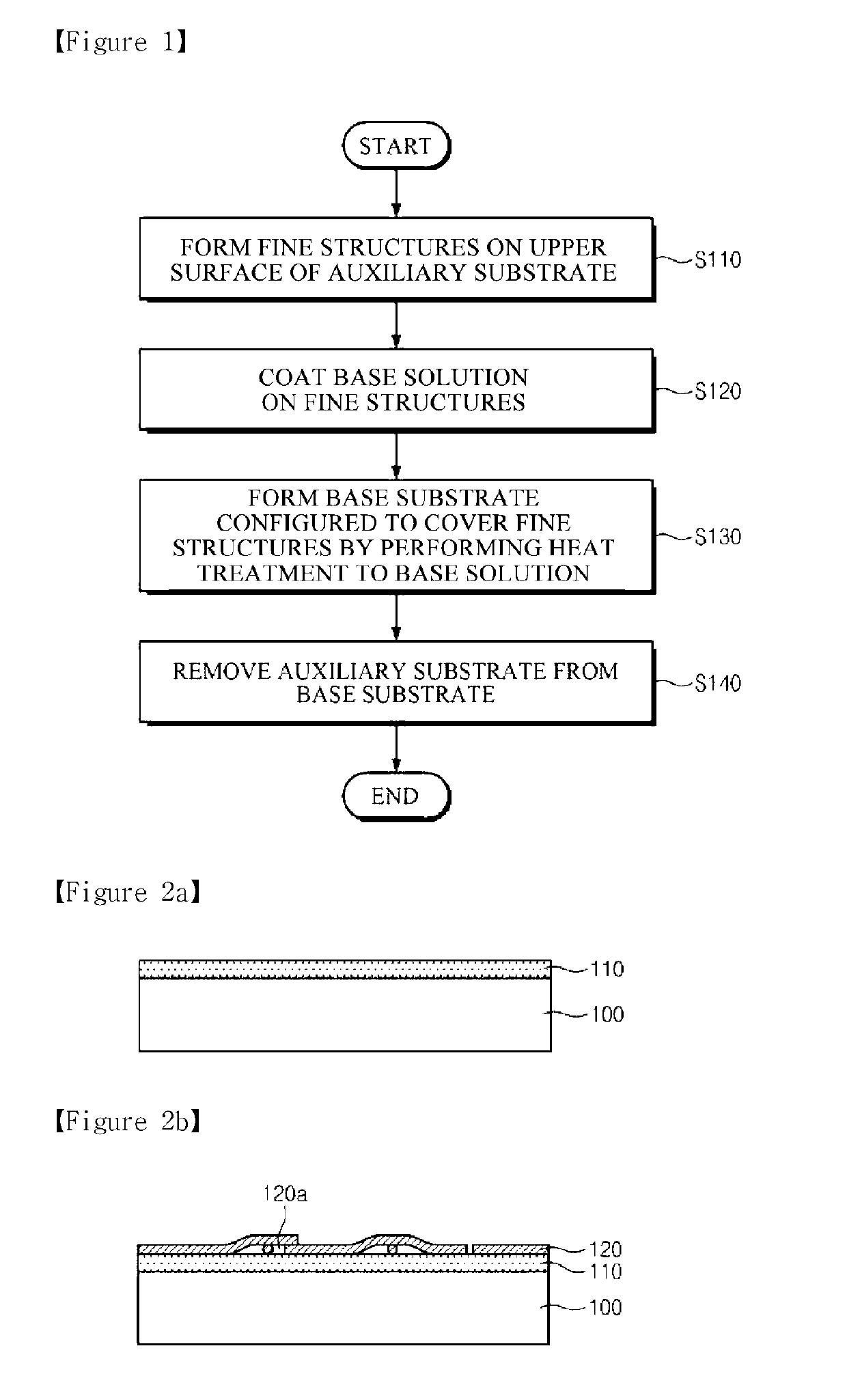
[0008]An object to be achieved by the present disclosure is to provide a substrate including nano / micro structures with a minimized surface roughness and a method for manufacturing the same.

[0009]Another object to be achieved by the present disclosure is to provide a substrate including nano / micro structures with high reliability and a method for manufacturing the same.

[0010]Yet another object to be achieved by the present disclosure is to provide a substrate including flexible nano / micro structures and a method for manufacturing the same.

[0011]Still another object to be achieved by the present disclosure is to provide a substrate including transparent and conductive nano / micro structures and a method for manufacturing the same.

[0012]Still another object to be achieved by the present disclosure is to provide a refining method and a refining apparatus for a nano / micro structure with high reliability.

[0013]Still another object to be achieved by the present disclosure ...


PUM

PropertyMeasurementUnit
temperatureaaaaaaaaaa
surface roughnessaaaaaaaaaa

Abstract

Provided is a manufacturing method for a substrate having a microstructure. The manufacturing method for a substrate having a microstmcture comprises the steps of: forming a microstructure on the upper surface of an auxiliary substrate; coating a base solution on the microstructure; forming a base substrate covering the microstructure by heattreating the base solution; and removing the auxiliary substrate from the base substrate.

Description

TECHNICAL FIELD[0001]The present disclosure relates to a substrate including nano / micro structures, a method for manufacturing the same, a method for refining a nano / micro structure, a method for manufacturing a nano / micro structure network, and a manufacturing apparatus therefor.BACKGROUND ART[0002]A micro / nano structure having a size of several nm to several hundred nm is manipulated and controlled in nano scale. Thus, new physical / chemical properties different from those of existing materials can be expected. Therefore, the micro / nano structure has been attracting a lot of attention as a next-generation material which can overcome the limitations of the existing materials.[0003]Such a micro / nano structure is one type of core new material that provides a foundation for use in technologies of various fields such as organic light emitting elements, liquid crystal displays, touch panels, or solar cells. Generally, a micro / nano structure is manufactured to various sizes by a chemical ...

Claims


Application Information

Patent Timeline
Patent Type & Authority Applications(United States)
IPC IPC(8): B29C41/20B29C37/00
CPCB29C41/20B29C37/0067B29C41/14B29C41/12B29K2105/0073B29C41/08B29C41/36B29L2031/756B05D1/00B05D3/002B05D3/007B05D3/02B05D5/04B05D5/12H05K3/12
Inventor KIM, TAEWHANCHOO, DONGCHULLEE, JUNGYU
Owner LG DISPLAY CO LTD
Why Eureka
Try Eureka