Etching solution composition, method for etching multilayer film, and method for manufacturing display device

A technology of composition and etching solution, applied in the direction of semiconductor/solid-state device manufacturing, electric solid-state device, semiconductor device, etc., can solve the problems of deterioration of operating environment, dissolution of resist, change of etching rate, etc., to prevent etching residue or precipitation The effect of reducing the amount of waste and waste liquid, and maximizing the linearity

A technology of composition and etching solution, applied in the direction of semiconductor/solid-state device manufacturing, electric solid-state device, semiconductor device, etc., can solve the problems of deterioration of operating environment, dissolution of resist, change of etching rate, etc., to prevent etching residue or precipitation The effect of reducing the amount of waste and waste liquid, and maximizing the linearity

CN106795633BActive Publication Date: 2021-02-05SAMYOUNG PURE CHEM +2

Image

  • Etching solution composition, method for etching multilayer film, and method for manufacturing display device
  • Etching solution composition, method for etching multilayer film, and method for manufacturing display device
  • Etching solution composition, method for etching multilayer film, and method for manufacturing display device

Examples


manufacture example 1

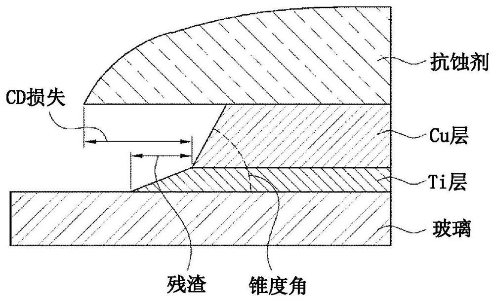
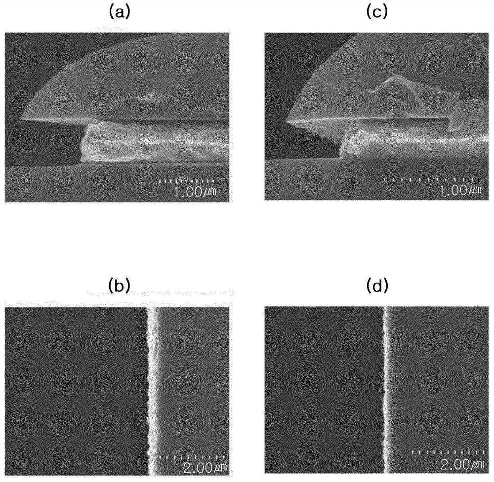
[0112] Production example 1: Fabrication of titanium / copper / titanium / glass substrate

[0113] A layer made of titanium (metal) is formed by sputtering titanium on a glass substrate (size: 150mm×150mm) Next, a layer made of copper (metal) is formed by sputtering copper After that, a layer made of titanium (metal) is formed by sputtering titanium Thus, a three-layer film structure of titanium / copper / titanium is produced. A resist was applied thereto, a line pattern mask (line width: 20 μm) was exposed and transferred, and developed to form a resist pattern, thereby producing a titanium / copper / titanium / glass substrate.

manufacture example 2

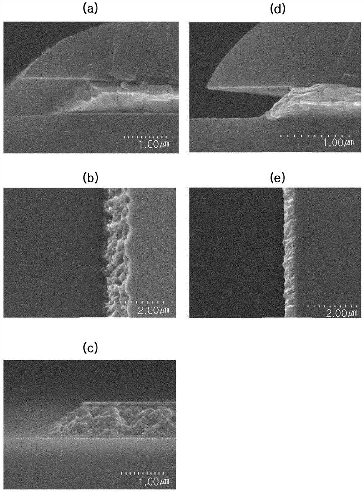
[0114] Production example 2: Production of copper / titanium / glass substrate

[0115] A layer made of titanium (metal) is formed by sputtering titanium on a glass substrate (size: 150mm×150mm) Next, a layer made of copper (metal) is formed by sputtering copper In this way, a copper / titanium 2-layer structure is produced. A resist was applied thereto, a line-shaped pattern mask (line width: 20 μm) was exposed and transferred, and developed to form a resist pattern, thereby producing a copper / titanium / glass substrate.


PUM


Abstract

The present invention relates to an etching solution composition, an etching method for a multilayer film, and a method for manufacturing a display device, wherein the etching solution composition of the present invention comprises: (A) a supply source of copper ions; (B) having 1 in the molecule An organic acid ion supply source of more than two carboxyl groups; (C) a fluoride ion supply source; (D) an etch regulator, a surface oxidation power enhancer, or a combination thereof as a first additive; and (E) as a second additive of surfactants.

Description

technical field [0001] The present invention relates to an etchant composition, a method for etching a multilayer film, and a method for manufacturing a display device. For example, it relates to an etchant composition that can be used to etch a multilayer film containing copper and titanium, an etching method for a multilayer film containing copper and titanium using the etchant composition, and an etching method using the etchant composition A method of manufacturing a display device. Background technique [0002] Conventionally, aluminum or an aluminum alloy is generally used as a wiring material for a display device such as a flat panel display. However, in the recent increase in size and resolution of displays, the problem of signal delay due to characteristics such as wiring resistance occurs in aluminum-based wiring materials, making it difficult to achieve uniform screen display. [0003] Therefore, research has been conducted on wiring mainly composed of copper, w...

Claims


Application Information

Patent Timeline
05 Feb 2021
Publication
CN106795633B
IPC
C23F1/16; C23F1/30; C23F1/20
CPC
C23F1/16; C23F1/20; C23F1/30; C23F1/18; C23F1/26; H01L27/124; H01L21/32134; H01L27/1259
Inventors
全重翼; 印致成