
Method for performing access control in a memory device, associated memory device and controller thereof

Active Publication Date: 2019-05-30
SILICON MOTION INC (TW)
View PDF0 Cites 1 Cited by
  • Summary
  • Abstract
  • Description
  • Claims
  • Application Information

AI Technical Summary

Benefits of technology

The present invention aims to provide a method for accessing a memory device with optimal performance without causing any side effects. This method can properly control access to data while performing data protection, even with limited hardware resources. Implementing this invention will not significantly increase overall costs and can solve existing problems in the related art without introducing additional costs. Overall, this invention achieves optimal performance of the memory device without causing any side effects.

Problems solved by technology

Improving access control of memories in these portable memory devices remains an issue to be solved in the art, however.
The MLC flash memory does have instability issues, however.
Memory devices inevitably have certain deficiencies, even those with the above management mechanism.
For example, a hardware mechanism designed in response to some types of data protection requirements can be very complicated.
In another example, massive data accessing designed in response to some types of data protection requirements may lower the overall efficiency of memory devices.

Method used


Image

  • Method for performing access control in a memory device, associated memory device and controller thereof
  • Method for performing access control in a memory device, associated memory device and controller thereof
  • Method for performing access control in a memory device, associated memory device and controller thereof

Examples


Embodiment Construction

I. Memory System

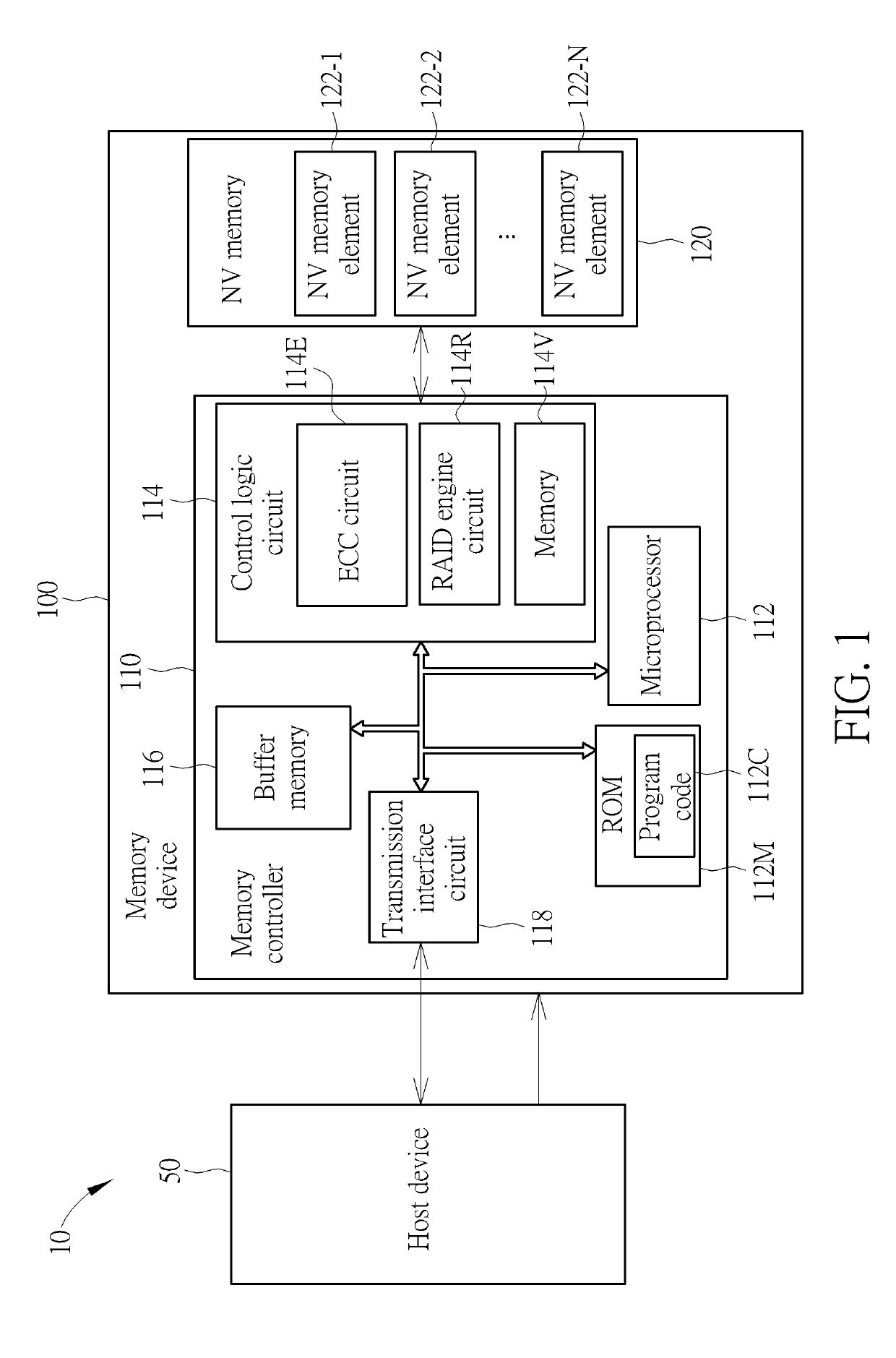
[0025]Refer to FIG. 1, which is a diagram illustrating a memory device 100 and a host device 50 according to a first embodiment of the present invention, wherein the electronic device 10 may comprise the host device 50 and the memory device 100. Examples of the memory device 100 may comprise (but are not limited to): a portable memory device (e.g. a memory card conforming to the SD / MMC, CF, MS, or XD specification), or a solid state drive (SSD). Further, examples of the host device 50 may comprise (but are not limited to): a multifunctional mobile phone, tablet, wearable device, and personal computer (e.g. a desktop computer or a laptop computer). According to this embodiment, the memory device 100 may comprise a controller such as a memory controller 110, and may further comprise a non-volatile (NV) memory 120, wherein the controller is arranged to access the NV memory 120, and the NV memory 120 is arranged to store information. The NV memory 120 may comprise a plur...


PUM


Abstract

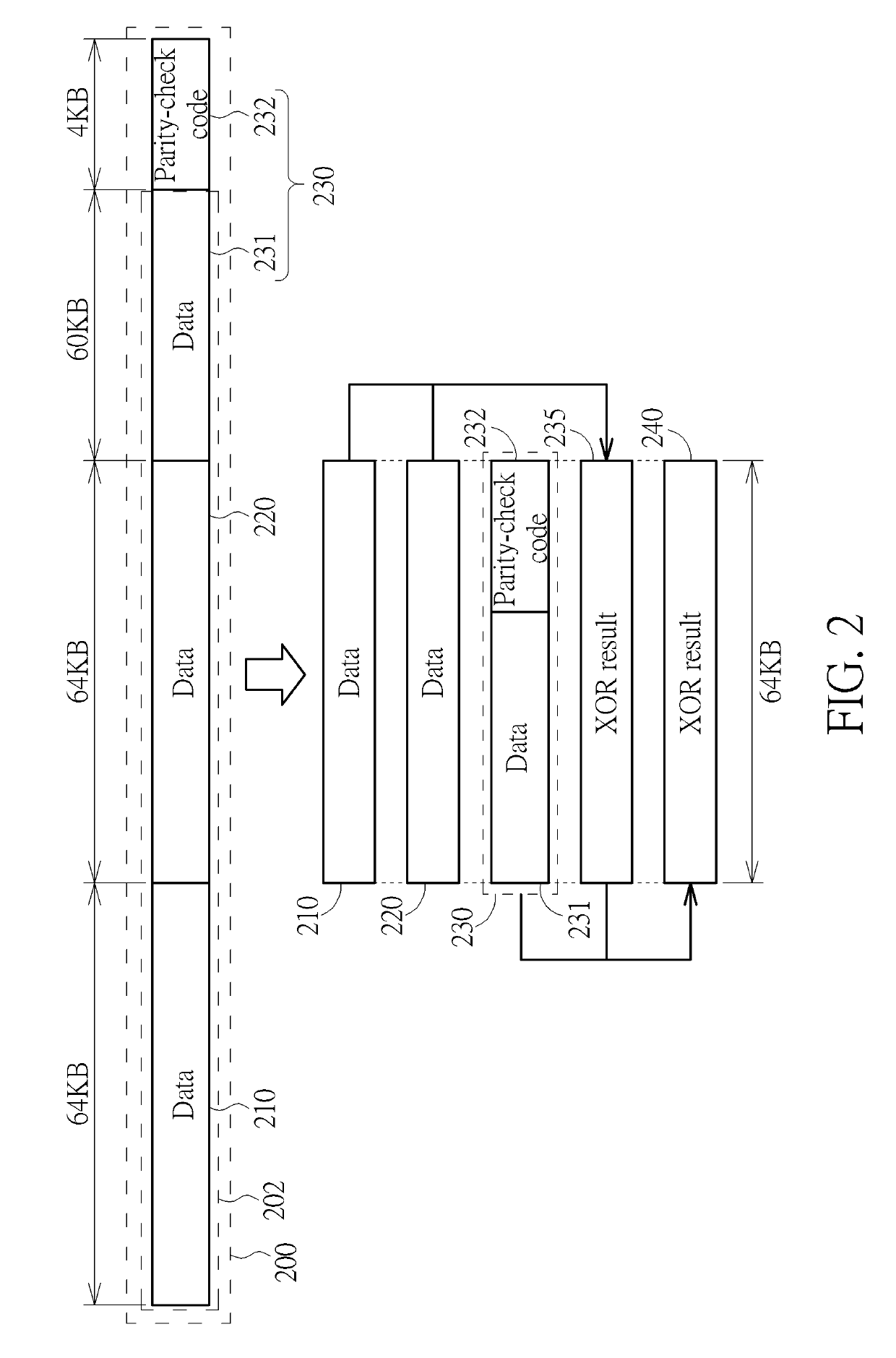
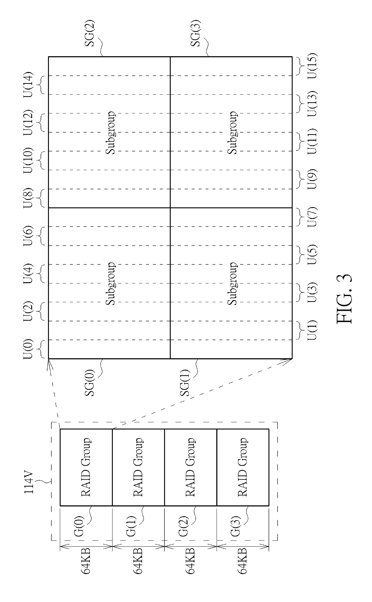
A method for performing access control in a memory device, the associated memory device and the controller thereof are provided. The method includes: according to at least one predetermined arrangement pattern, writing a plurality of sets of symbols into a plurality of storage regions of a memory as a plurality of redundant array of independent disks (RAID) groups, respectively; and utilizing a RAID engine circuit in the memory device to perform a plurality of operations related to data protection, such as: determining a series of reading patterns corresponding to the predetermined arrangement pattern; according to a reading pattern of the series of reading patterns, reading a plurality of symbols from each RAID group of the RAID groups; and performing exclusive-OR (XOR) operations on the symbols to convert the symbols into at least one XOR result, for performing data protection.

Description

BACKGROUND OF THE INVENTION1. Field of the Invention[0001]The present invention relates to access control of flash memories, and more particularly, to a method for performing access control in a memory device, the associated memory device and controller thereof.2. Description of the Prior Art[0002]Developments in memory technology have enabled the wide application of portable memory devices, such as memory cards conforming to SD / MMC, CF, MS and XD specifications, solid state drives, or embedded storage devices conforming to the UFS and EMMC specifications. Improving access control of memories in these portable memory devices remains an issue to be solved in the art, however.[0003]NAND flash memories may comprise single level cell (SLC) and multiple level cell (MLC) flash memories. In an SLC flash memory, each transistor used as a memory cell may have either of two electrical charge values respectively corresponding to logic values 0 and 1. In comparison, the storage ability of each ...

Claims


Application Information

Patent Timeline
IPC IPC(8): G06F11/10G06F3/06
CPCG06F11/1076G06F3/0619G06F3/0644G06F3/0689G06F3/0679G06F3/0688G06F3/0659G06F3/0656
Inventor CHENG, CHIAO-WEN
Owner SILICON MOTION INC (TW)
Learn More