

Organic light-emitting display device
a display device and organic technology, applied in semiconductor devices, diodes, instruments, etc., can solve problems such as non-uniform image display, and achieve the effect of preventing the threshold voltage of a thin film transistor
- Summary
- Abstract
- Description
- Claims
- Application Information
AI Technical Summary
Benefits of technology
Problems solved by technology
Method used
Image

Examples
Embodiment Construction
[0016]Embodiments of the present disclosure will be described in detail with reference to the attached drawings.
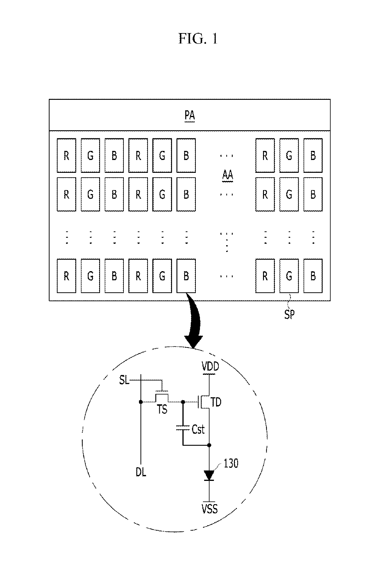
[0017]FIG. 1 is a plan view illustrating an organic light-emitting display device according to the present disclosure.
[0018]The organic light-emitting display device shown in FIG. 1 includes an active area AA and a pad area PA.
[0019]A plurality of pads through which driving signals are supplied to scan lines SL, data lines DL, a high voltage (VDD) supply line and a low voltage (VSS) supply line arranged in the active area AA is formed in the pad area PA.
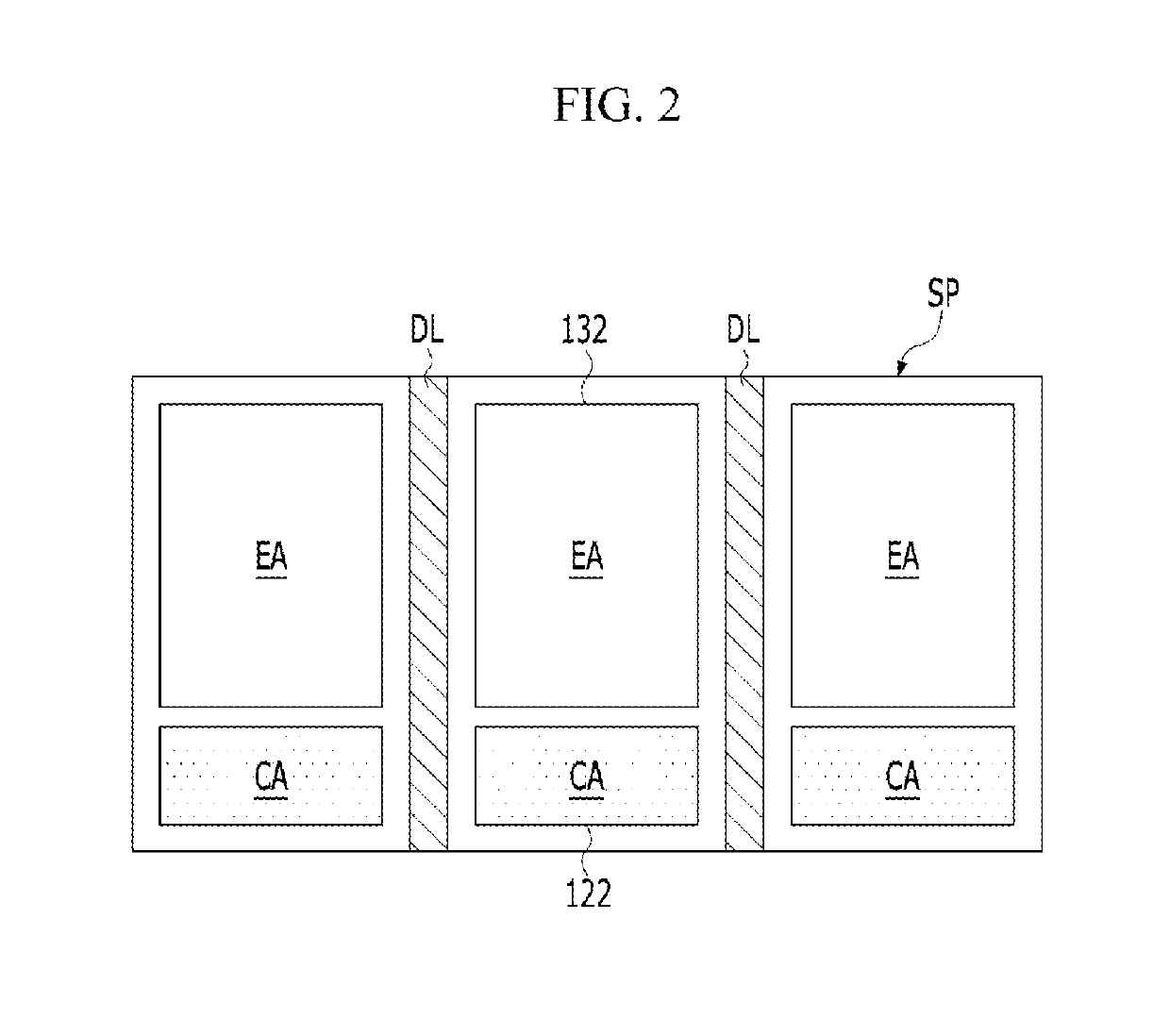
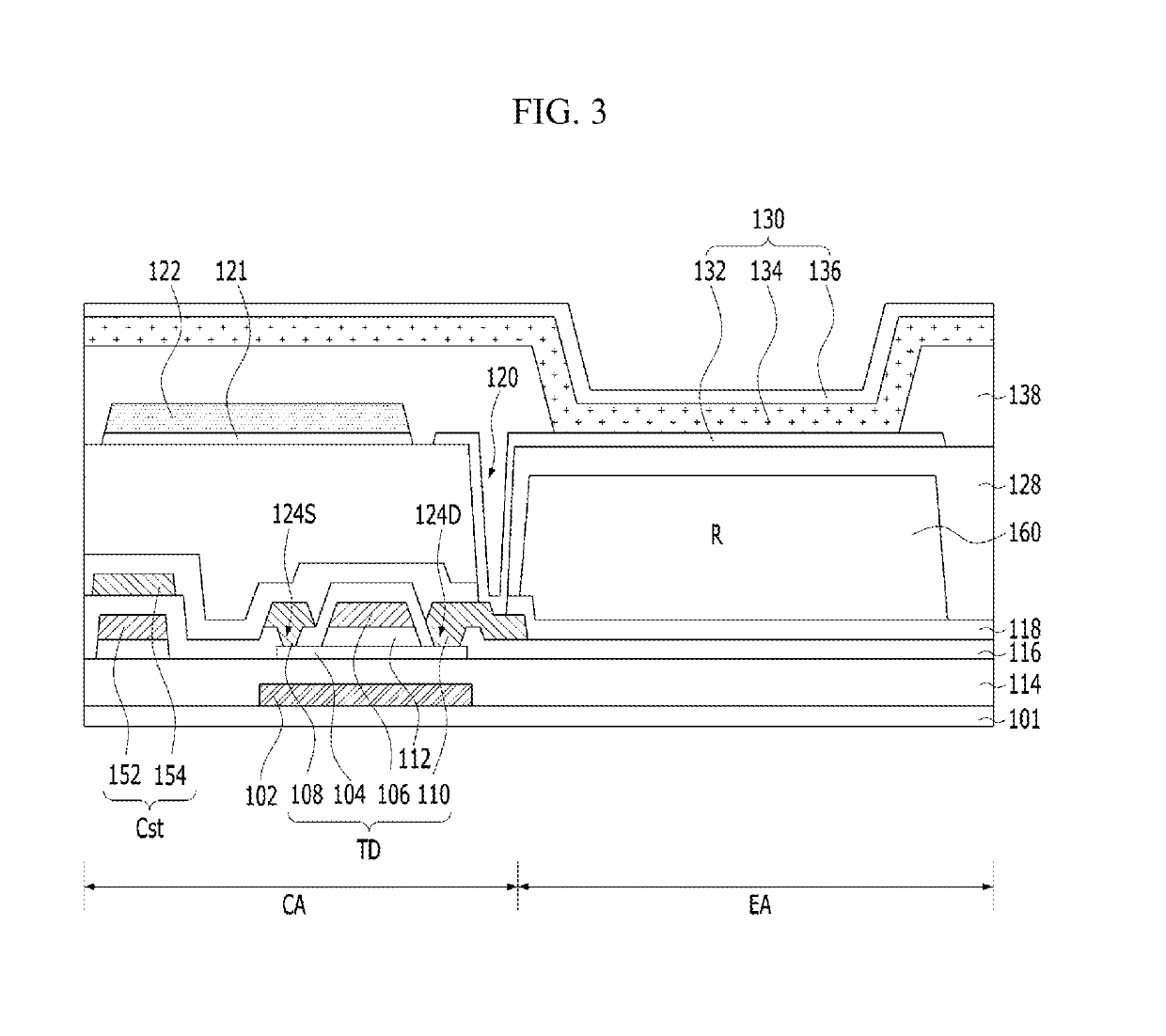
[0020]The active area AA displays an image through unit pixels including light-emitting elements 130. A unit pixel is composed of red (R), green (G) and blue (B) sub-pixels or red (R), green (G), blue (B) and white (W) sub-pixels. Each sub-pixel includes an emission element 130 and a pixel driving circuit for independently driving the emission element 130. Here, the emission element is disposed in an emission area of each s...
PUM
 Abstract
Description
Claims
Application Information