

Method for manufacturing a mask blank substrate, method for manufacturing a mask blank, method for manufacturing a transfer mask, method for manufacturing a semiconductor device, a mask blank substrate, a mask blank, and a transfer mask
Active Publication Date: 2019-07-25
HOYA CORP
View PDF2 Cites 0 Cited by
- Summary
- Abstract
- Description
- Claims
- Application Information
AI Technical Summary
Benefits of technology
The invention provides a method for making a mask blank substrate or mask blank that can reduce focus errors when exposed using a high NA exposure apparatus. This results in a more precise and accurate transfer of the desired pattern during the manufacturing process.
Problems solved by technology
However, without adjusting a focus of a transfer mask face and a wafer face during scanning, a focus error occurs and causes a significant deviation of an image forming position from the best focus so that resolution of the transfer pattern on the resist film is significantly reduced.
Method used
View moreImage
Smart ImageViewing Examples

Examples
examples
[0107]The embodiments of this invention are described in greater detail below together with examples.
Login to View More PUM
 Abstract
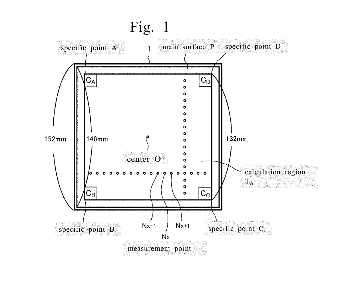
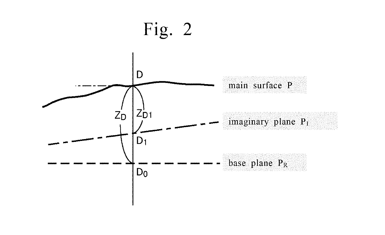
A mask blank substrate and a method for selecting a mask blank substrate wherein a square calculation region is set on the main surface of the substrate. Specific points are set at the corner portions of the calculation region. The heights of the specific points from a reference plane are acquired, an imaginary plane passing through three of the specific points is set, an intersection between the imaginary plane and a perpendicular line that passes through the remaining of the specific points and that is perpendicular to the reference plane is set, and the distance between the remaining of the specific points and the intersection is calculated. A substrate in which the distance satisfies a predetermined reference value is selected as a mask blank substrate.
Description
TECHNICAL FIELD[0001]This invention relates to a method for manufacturing a mask blank substrate, a method for manufacturing a mask blank, a method for manufacturing a transfer mask, a method for manufacturing a semiconductor device, a mask blank substrate, a mask blank, and a transfer mask.BACKGROUND ART[0002]In recent years, an increase in high NA (Numerical Aperture) in an exposure apparatus using an ArF exposure light is in progress to deal with the miniaturization of semiconductor devices, and further increase in high NA is in progress by introduction of liquid immersion exposure technique. Higher NA in an exposure apparatus causes improvements in resolution in exposure-transferring a fine pattern provided on a transfer mask on a resist film on a wafer. In a step-and-scanning type exposure apparatus, an exposure light scans over a transfer mask and a wafer so as to exposure-transfer a transfer pattern on the transfer mask on a resist film on the wafer.[0003]However, without adj...
Claims
Login to View More Application Information
Patent Timeline
 IPC IPC(8): G03F1/32G03F1/60G03F7/20
CPCG03F1/32G03F1/60G03F7/70716G03F1/50
InventorTANABE, MASARU
OwnerHOYA CORP