


Quick Research
Generate reliable direction feasibility study reports for your R&D in just a few steps.

Technical Q&A
Discover and master advanced knowledge NOW. Basics, ideas, possibilities, all at once.

Find Solutions
As an expert in R&D theories, this can generate solutions to your technical problems instantly.

Evaluate Feasibility
Analyze your overall solution with one click, know your potential R&D risks in advance.

Monitor Landscape
Get weekly tech updates, stay abreast of the latest tech innovations and key insights.
High Definition Microdroplet Printer
a printer and high-definition technology, applied in the field of high-definition micro-droplet printers, can solve the problem of limited ability to perform measurements over extended periods of tim
- Summary
- Abstract
- Description
- Claims
- Application Information
AI Technical Summary
Benefits of technology
Problems solved by technology
Method used
Image

Examples
example 1
Fabrication and Testing of Microfluidic Nozzle and Patterned Electrode Substrate
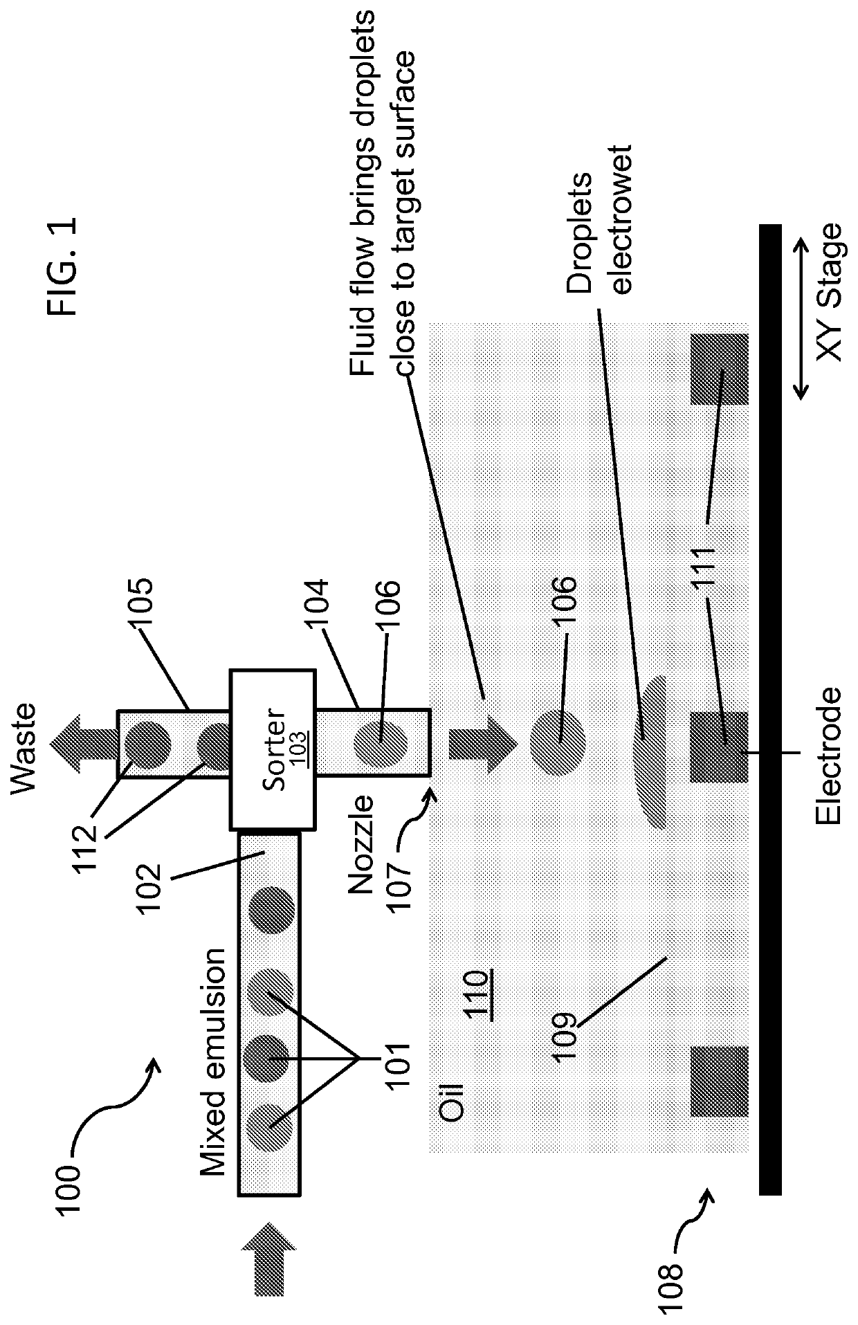
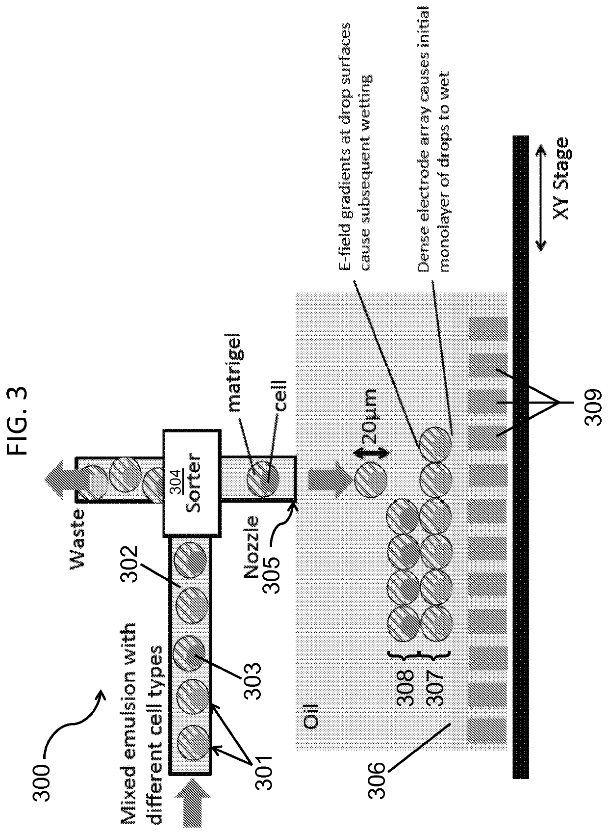
[0674]A microdroplet printing system was built and tested using the scheme displayed in FIG. 8. A droplet microfluidic print head, including a compact microfluidics droplet sorter modified with an exit nozzle, is suspended above the stage of an inverted microscope. Droplets flowing through the sorter are fluorescently labeled and detected within the device by a laser coupled to external detection optics. When a desired droplet is detected, it is actively sorted to the nozzle and directed to a target surface. A constant background flow of carrier fluid (oil) brings the droplet in close contact with the dielectrophoretic trap. A customized substrate with biopolar electrodes patterned into its surface is placed on the xy stage of the microscope and serves as a target for the deposition of droplets. Specific regions on the substrate with high electric field gradients serve as dieletrophoretic traps for dropl...
example 2
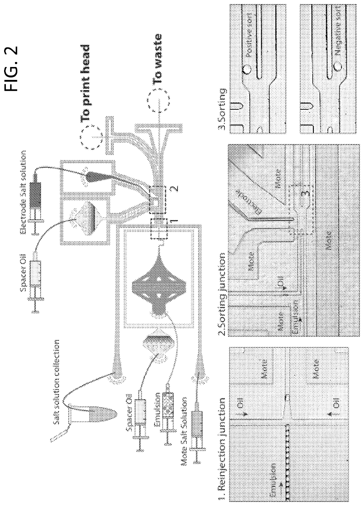
Improved Sorting Architecture for High-Speed Sorting of Microdroplets
[0679]Described herein is a microfluidic design that permits 30 kHz droplet sorting with >99% accuracy. This tenfold rate increase compared to the fastest available droplet sorters enables ˜108 droplets to be sorted per hour and over a billion per day. Indeed, with the described architecture, sorting speed is not limited by the physical mechanism of sorting (even at Ca˜1) but rather by the electronics that detect the droplets; with faster electronics, even faster sorting is anticipated.
[0680]The devices were fabricated using soft lithography of poly(dimethylsiloxane) (PDMS) moulded from device masters. The masters were created from two sequential layers (11 μm and 19 μm thick) of photoresist (MicroChem, SU-8 3010) spun onto a silicon wafer. Uncured PDMS consisting of a 10:1 polymer to cross-linker mixture (Dow Corning, Sylgard 184) was poured onto the master, degassed, and baked at 85° C. for 2 hours. The PDMS moul...
PUM
 Abstract
Description
Claims
Application Information
 - R&D Engineer
- R&D Manager
- IP Professional
- Industry Leading Data Capabilities
- Powerful AI technology
- Patent DNA Extraction
Browse by: Latest US Patents, China's latest patents, Technical Efficacy Thesaurus, Application Domain, Technology Topic, Popular Technical Reports.
© 2024 PatSnap. All rights reserved.Legal|Privacy policy|Modern Slavery Act Transparency Statement|Sitemap|About US| Contact US: help@patsnap.com