Electronic device and noise removal system
a technology of electronic devices and noise removal, applied in the direction of pulse manipulation, pulse technique, electrical apparatus, etc., can solve problems such as fatal errors, and achieve the effect of removing glitch noise and removing glitch noise from input signals
- Summary
- Abstract
- Description
- Claims
- Application Information
AI Technical Summary
Benefits of technology
Problems solved by technology
Method used
Image

Examples
first embodiment
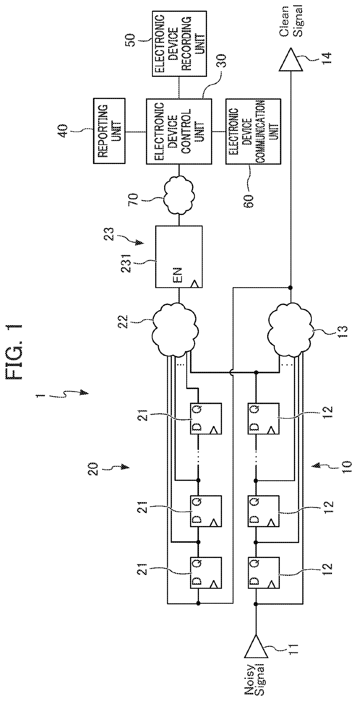
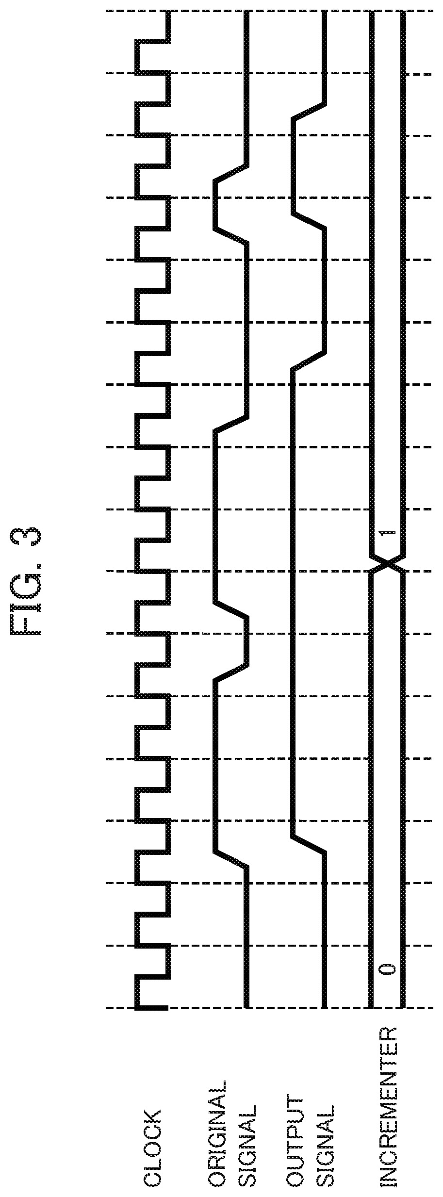
[0028]FIG. 1 is a circuit diagram showing an electronic device 1 according to a first embodiment of the present disclosure. The electronic device 1 has a function of removing glitches included in signals. It should be noted that, in the following explanation, “glitch noise” and “glitch” may be explained simply as “glitch”.
[0029]The electronic device 1 includes: a glitch removal circuit 10 which removes glitches from the inputted signal; a count unit 20 which counts a number of times that the glitch removal circuit 10 removed glitches; an electronic device control unit 30 which performs control based on a count number of the count unit 20; a reporting unit 40 which, in a case where the count number of the count unit 20 exceeds a predetermined threshold value, reports this event; an electronic device recording unit 50 which leaves the count number of the count unit 20 in a log periodically or when a predetermined event occurs; and an electronic device communication unit 60 which commu...
second embodiment
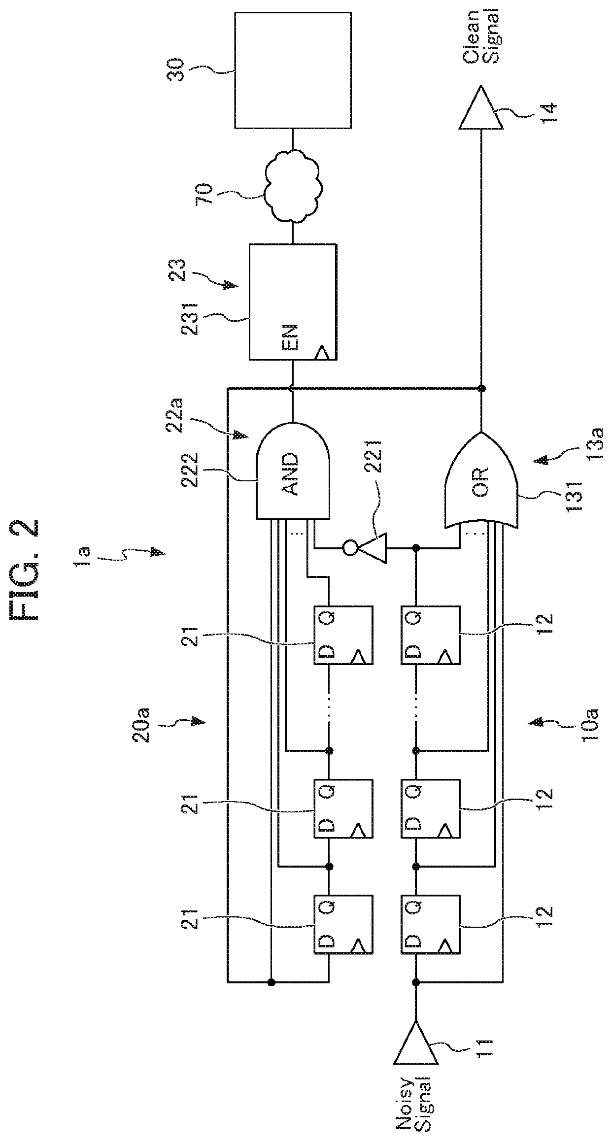
[0055]FIG. 2 is a circuit diagram showing an electronic device 1a according to a second embodiment of the present disclosure. The electronic device 1 is a device which removes glitches in a low level direction appearing in the input signal of high level. It should be noted that, in the following explanation, the same reference symbols are attached to constituent elements which are the same as in the previously explained embodiment, and redundant explanations may be omitted.
[0056]The electronic device 1a of the present embodiment includes: a glitch removal circuit 10a which removes glitches from the inputted signal; a count unit 20a which counts a number of times that the glitch removal circuit 10a removed glitches; and an electronic device control unit 30 which performs control based on the count number of the count unit 20a.
[0057]The electronic device control unit 30 in the electronic device 1a of the present embodiment is similar to the electronic device control unit 30 of the el...
third embodiment
[0073]FIG. 4 is a circuit diagram showing an electronic device 1b according to a third embodiment of the present disclosure. The electronic device 1b is a device which removes a glitch in the high level direction appearing in the input signal which is low level.
[0074]The electronic device 1b of the present embodiment includes: a glitch removal circuit 10b which removes a glitch from the inputted signal; a count unit 20b which counts a number of times that the glitch removal circuit 10b removed glitches; and an electronic device control unit 30 which performs control based on the count number of the count unit 20b.
[0075]The electronic device control unit 30 in the electronic device 1b of the third embodiment is similar to the electronic device control unit 30 in the electronic device 1 of the first embodiment.
[0076]The glitch removal circuit 10b includes the signal input terminal 11, n stages (n is an integer of 1 or more) of original signal delay elements 12, an output signal gener...
PUM
 Abstract
Description
Claims
Application Information
 - R&D Engineer
- R&D Manager
- IP Professional
- Industry Leading Data Capabilities
- Powerful AI technology
- Patent DNA Extraction
Browse by: Latest US Patents, China's latest patents, Technical Efficacy Thesaurus, Application Domain, Technology Topic.
© 2024 PatSnap. All rights reserved.Legal|Privacy policy|Modern Slavery Act Transparency Statement|Sitemap