CDS capable sensor with photon sensing layer on active pixel circuit

a photon sensing layer and sensor technology, applied in the field of cmos sensors, can solve the problems of incomplete charge transfer, inability to fabricate the travel path in real practice, etc., and achieve the effect of fine tuning the overall sensor performance, eliminating clock noise, and eliminating clock nois

Inactive Publication Date: 2007-12-13
E PHOCUS
View PDF1 Cites 71 Cited by
  • Summary
  • Abstract
  • Description
  • Claims
  • Application Information

AI Technical Summary

Benefits of technology

[0018] The present invention provides a MOS or CMOS based active pixel sensor with special sampling features to substantially eliminate clock noise. The sensor includes an array of pixels fabricated in or on a substrate, each pixel defining a charge collection node on which charges generated inside a photodiode region are collected, a charge integration node, at which charges generated in said pixel are integrated to produce pixel signals, a charge sensing node from which reset signals and the pixel signals are sensed. In preferred embodiments the sensor includes a continuous electromagnetic radiation detection structure located above the pixel circuits providing a photodiode region for each pixel. The sensor includes integrated circuit elements adapted to maintain voltage potentials at the charge collection nodes substantially constant during charge integration cycles. The sensor also includes integrated circuit elements having electrical capacitance adapted to store charges providing an electrical potential at the charge integration node. In preferred embodiments this is a pinned diode. The sensor also includes a transfer switch to transfer charges from the charge integration node to the charge sensing node. The sensor also includes integrated circuit elements having electrical capacitance adapted to store charges providing an electrical potential at the charge sensing node. The sensor also includes integrated circuit elements adapted to reset the charge sensing node and the charge integration node, integrated circuit elements adapted to convert the charges on the charge sensing node into electrical signal, and integrated circuit elements adapted to readout electrical signals generated in the pixels.
[0019] One of the very important features of preferred embodiments of this invention is that the charge integration node and charge sensing node are separated from each other. This feature permits correlated double sampling that basically eliminate clock noise as a problem.
[0020] Another important feature of preferred embodiments of this invention is that Applicant also separates the charge collection node from the charge integration node. In this separation Applicant preferably uses a transistor whose gate is held at a substantially constant voltage, about 1.2 V, during the charge integration cycle. The applicant makes this bias voltage programmable in the range of 0.8V to 1.6V to fine tune the overall sensor performance. This transistor maintains the voltage at the charge collection node at a constant value. The charge collection node is considered electrically short to the pixel electrode. This constant voltage not only substantially eliminates pixel crosstalk but also eliminates the need to use the built-in capacitance of the photodiode to store signal charges. When the charge integration node is reset at the beginning of the integration cycle, this constant gate bias transistor allows current flowing from the charge integration node to the charge collection node until the charge collection node is charged up to slightly (a few tenths of a volt) below the constant gate bias. The capacitor associated with the integration node is rese

Problems solved by technology

This travel path can not be fabricated with perfection in rea

Method used


Image

  • CDS capable sensor with photon sensing layer on active pixel circuit
  • CDS capable sensor with photon sensing layer on active pixel circuit
  • CDS capable sensor with photon sensing layer on active pixel circuit

Examples


Embodiment Construction

First Preferred Embodiment—Five Transistor Design

[0031] A first preferred embodiment of the present invention is shown in FIG. 4 and FIG. 5. This embodiment combines features of the prior art POAP technology, pinning technology and correlated double sampling, all discussed in the background section to provide a sensor with approximately 100 percent packing factor and substantially zero clock noise. The result is a sensor with approximately 100 percent improvement in sensitivity over typical prior art CMOS sensors and a 40 percent improvement over prior art POAP sensors.
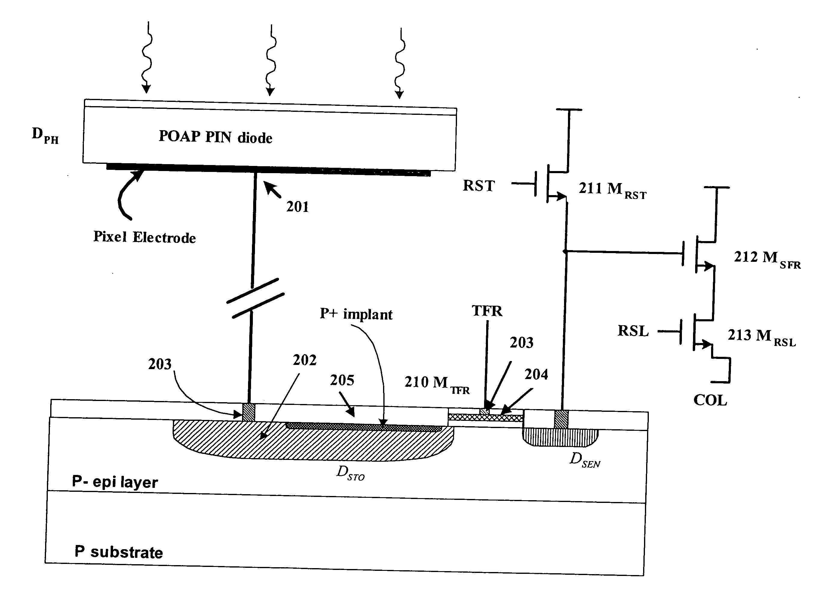
Pixel Structure

[0032] As shown if FIG. 5 a first preferred embodiment includes a four layer POAP type photodiode 300 covering all pixels in the pixel array. The four layers are an n-doped layer 302, an intrinsic i-layer 304, a p-doped layer 306 and an indium-tin-oxide (ITO) layer 308. The POAP structure also includes an electrode 310 for each individual pixel in the pixel array. A silicon oxide insulating layer 22...


PUM


Abstract

A MOS or CMOS based active pixel sensor with special sampling features to substantially eliminate clock noise. The sensor includes an array of pixels fabricated in or on a substrate, each pixel defining a charge collection node on which charges generated inside a photodiode region are collected, a charge integration node, at which charges generated in said pixel are integrated to produce pixel signals, a charge sensing node from which reset signals and the pixel signals are sensed. In preferred embodiments the sensor includes a continuous electromagnetic radiation detection structure located above the pixel circuits providing a photodiode region for each pixel. The sensor includes integrated circuit elements adapted to maintain voltage potentials of the charge integration nodes substantially constant during charge integration cycles. The sensor also includes integrated circuit elements having electrical capacitance adapted to store charges providing an electrical potential at the charge integration node. In preferred embodiments this is a pinned diode.

Description

CROSS REFERENCE TO RELATED APPLICATIONS [0001] This application is a continuation-in-part of U.S. patent applications Ser. No. 10 / 229,953 filed Aug. 27, 2002 and Ser. No. 10229,955 filed Aug. 27, 2002.[0002] The present invention relates to CMOS imaging sensors and in particular to such sensors with special sampling features. BACKGROUND OF THE INVENTION Prior Art Pinned Photodiode Sensors [0003] Pinned photodiodes sensors are well known in the prior art. Following are examples of patents describing CMOS sensors employing pinned photodiodes: U.S. Pat. Nos. 5,625,210; 5,880,495; 5,904,493; 6,297,070; 6,566,697; 6,967,120; and 7,115,855. All of these patents are incorporated herein by reference. Constant Gate Bias Transistors [0004] Operation of transistors with constant gate bias is a well known technique used to maintain the source voltage of a transistor at a constant value. For example, for n-type transistors operated with 3.3 supply voltage, a gate voltage at a about 0.7 volts (th...

Claims


Application Information

Patent Timeline
IPC IPC(8): H04N3/14
CPCH01L27/14634H01L27/14643H04N5/37457H04N5/3575H04N5/32H04N25/616H04N25/778
Inventor HSIEH, TZU-CHIANG
Owner E PHOCUS
Why Eureka
Try Eureka