Pixel and related organic light emitting diode display device

a technology of light-emitting diodes and display devices, which is applied in the direction of instruments, static indicating devices, etc., can solve the problems of unsatisfactory image quality and distorted stored data signals of oled display devices, and achieve the effect of satisfying the image quality of organic light-emitting diodes display devices

Active Publication Date: 2021-04-15
SAMSUNG DISPLAY CO LTD
View PDF0 Cites 11 Cited by
  • Summary
  • Abstract
  • Description
  • Claims
  • Application Information

AI Technical Summary

Benefits of technology

[0046]In embodiments, in a low frequency hold period, an off voltage level of at least one of a scan signal applied to a third transistor (e.g., a threshold voltage compensating transistor) and an initialization signal applied to a fourth transistor (e.g., a gate initializing transistor) may be unequal to the voltage level in a normal frequency frame period. Advantageously, a voltage distortion of a gate node of a first transistor (e.g., a driving transistor) at low frequency driving may be compensated, and satisfactory image quality of the organic light emitting diode display device may be attained.

Problems solved by technology

When the OLED display device displays an image based on the stored data signals, the stored data signals may be distorted by leakage currents of transistors included in pixels of the OLED display device.
As a result, quality of images displayed by the OLED display device may be unsatisfactory.

Method used


Image

  • Pixel and related organic light emitting diode display device
  • Pixel and related organic light emitting diode display device
  • Pixel and related organic light emitting diode display device

Examples


Embodiment Construction

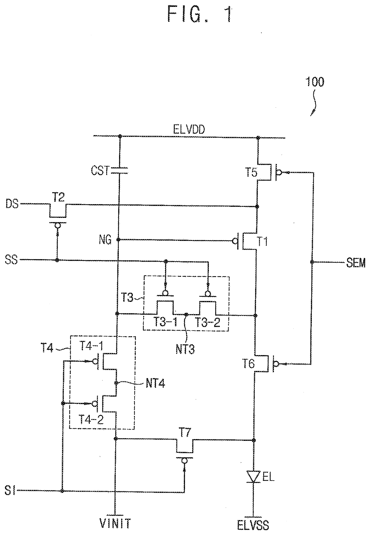
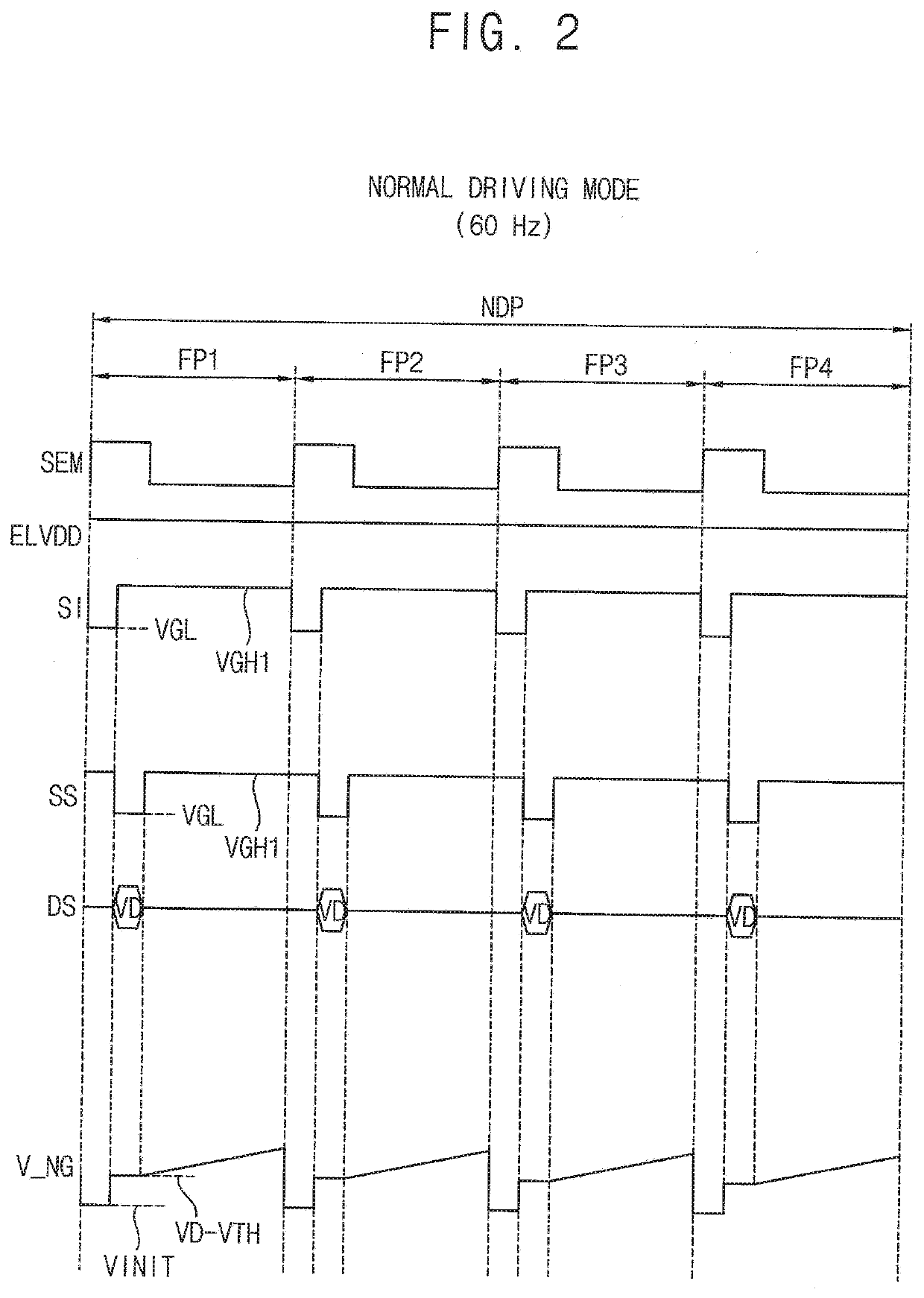
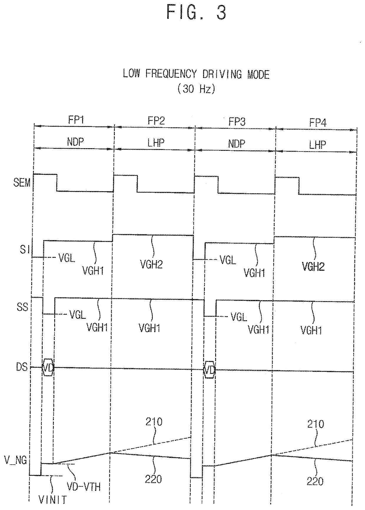
[0073]Embodiments are described with reference to the accompanying drawings. Although the terms “first,”“second,” etc. may be used to describe various elements, these elements should not be limited by these terms. These terms may be used to distinguish one element from another element. A first element may be termed a second element without departing from teachings of one or more embodiments. The description of an element as a “first” element may not require or imply the presence of a second element or other elements. The terms “first,”“second,” etc. may be used to differentiate different categories or sets of elements. For conciseness, the terms “first,”“second,” etc. may represent “first-type (or first-set),”“second-type (or second-set),” etc., respectively. The term “connect” or the term “couple” may mean “electrically connect” or “electrically connected through no intervening transistor.” The term “insulate” may mean “electrically insulate” or “electrically isolate.” The term “dr...


PUM

PropertyMeasurementUnit
driving frequencyaaaaaaaaaa
frequencyaaaaaaaaaa

Abstract

A pixel of a display device includes a capacitor; a light emitting diode; and first, second, third, and fourth transistors. The display device has a normal frequency mode and a low frequency mode. Two electrodes of the capacitor are respectively connected to a first voltage source and a gate node. A gate electrode of the first transistor is connected to the gate node. In a hold period in the low frequency mode, both the second and third transistors receive a scan signal, the third transistor diode-connects the first transistor, the fourth transistor receives an initialization signal and transfers an initialization voltage to the gate node, the scan signal is at a first off voltage level, and the initialization signal is at a second off voltage level unequal to the first off voltage level. The cathode of the light emitting diode is connected to a second voltage source.

Description

CROSS-REFERENCE TO RELATED APPLICATION(S)[0001]This application claims priority under 35 USC § 119 to Korean Patent Application No. 10-2019-0126965 filed on Oct. 14, 2019 in the Korean Intellectual Property Office (KIPO); the Korean Patent Application is incorporated by reference.BACKGROUND1. Field[0002]The technical field relates to a pixel of an organic light emitting diode display device and the organic light emitting diode display device.2. Description of the Related Art[0003]Reduction of power consumption may be desirable in an organic light emitting diode (OLED) display device employed in a portable device, such as a smartphone or a tablet computer. In order to reduce the power consumption of an OLED display device, the OLED display device may operate at a relatively low frequency driving when displaying a still image. When performing low frequency driving, the OLED display device may display an image based on stored data signals, thereby reducing the power consumption.[0004]W...

Claims


Application Information

Patent Timeline
Patent Type & Authority Applications(United States)
IPC IPC(8): G09G3/3258
CPCG09G3/3258G09G2330/028G09G2320/02G09G3/3208G09G3/3266G09G2300/0819G09G2300/0861G09G2300/0842G09G3/3233G09G2320/0214G09G2320/0233G09G2340/0435G09G2310/024G09G2300/0809G09G2310/0264
Inventor LEE, HYO JINKWON, SANGANROH, JIN YOUNGPARK, SEHYUK
Owner SAMSUNG DISPLAY CO LTD
Why Eureka
Try Eureka