Active matrix organic light-emitting diode display panel

a technology of organic light-emitting diodes and active matrix, which is applied in the field of display technology, can solve the problems of difficult to achieve the narrow upper bezel design of the active matrix organic light-emitting diode display panel, the brightness difference between the two rows is significant, and the design of the narrow upper bezel cannot be realized, so as to reduce the wiring space of the narrow upper bezel effectively.

Active Publication Date: 2021-07-15
WUHAN CHINA STAR OPTOELECTRONICS SEMICON DISPLAY TECH CO LTD
View PDF0 Cites 0 Cited by
  • Summary
  • Abstract
  • Description
  • Claims
  • Application Information

AI Technical Summary

Benefits of technology

[0010]In the present invention, the voltage lines and the scan lines are stacked in the concave area, so that the voltage lines overlap the scan lines to form an RC compensation capacitor. Since the voltage lines generally have a voltage with a relatively stable DC signal, the RC compensation capacitor formed by the voltage lines and the scan lines can achieve the purpose of RC compensation. Meanwhile, compared with the prior art, by reusing a wiring space of the voltage lines, the wiring space of the narrow upper bezel can be effectively reduced, thereby realizing the design of the narrow upper bezel. Further, the RC compensation value of each of the rows can be adjusted by adjusting an overlapping area of the polysilicon layers of the scan lines and the voltage lines, thereby reducing the display difference.

Problems solved by technology

The design of the concave active matrix organic light-emitting diode display panel is characterized by a large difference in a number of pixels between different rows of the concave area, especially the difference between the two rows of pixels at the boundary between the concave area and the display area, which eventually results in a significant difference in brightness between the two rows, and a phenomenon of split-screen between the concave area and the display area on the display.
However, since the RC compensation unit is generally placed on the upper bezel of the panel, due to the large number of the compensation units, it is difficult to achieve a narrow upper bezel, so that the design of the narrow upper bezel of the active matrix organic light-emitting diode display panel cannot be realized.

Method used


Image

  • Active matrix organic light-emitting diode display panel
  • Active matrix organic light-emitting diode display panel
  • Active matrix organic light-emitting diode display panel

Examples


Embodiment Construction

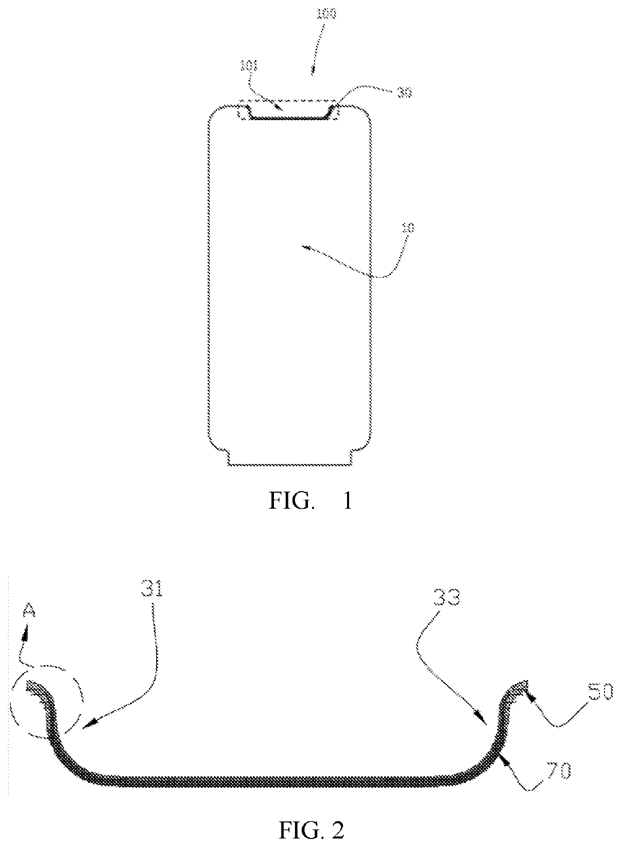
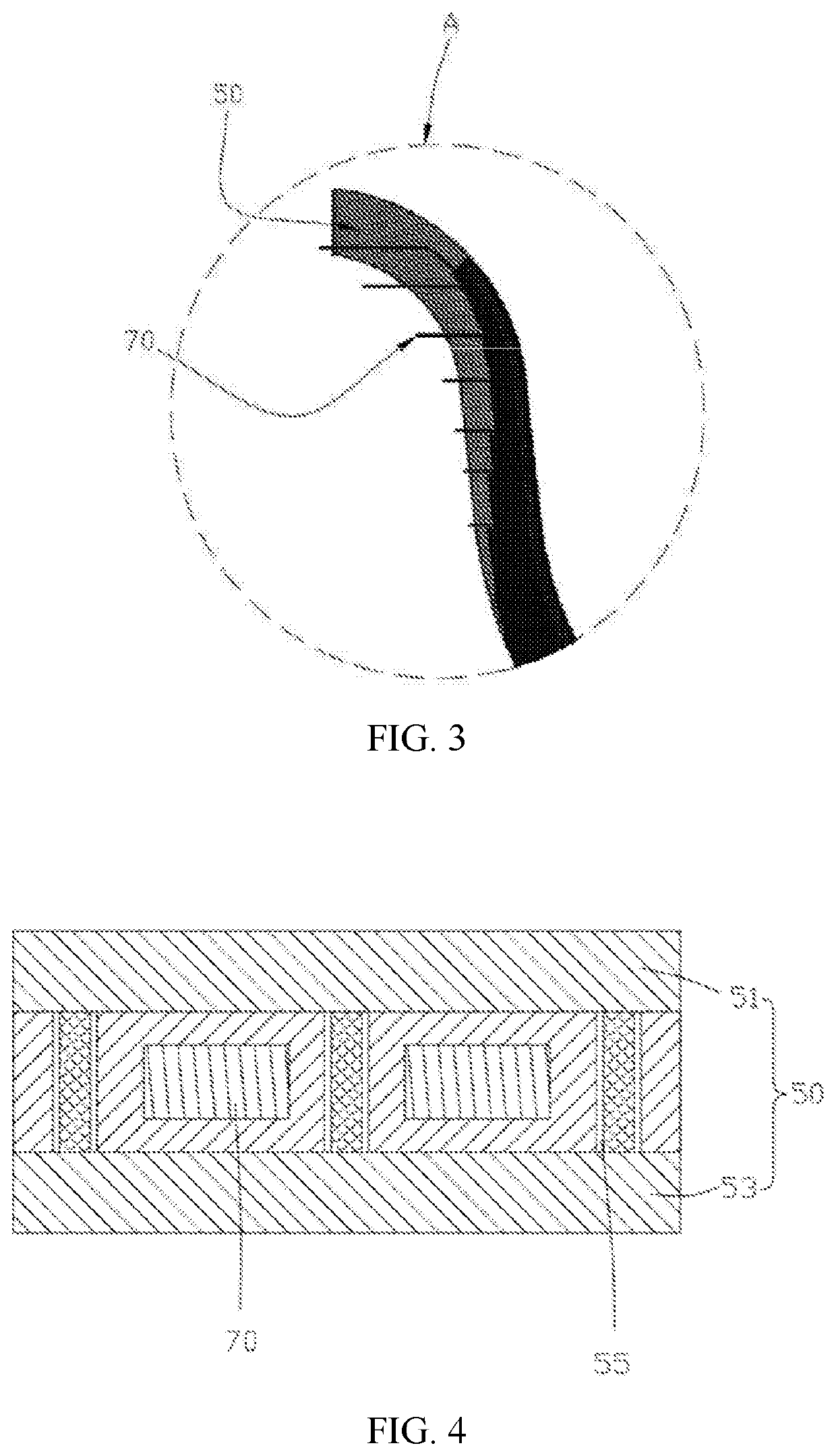
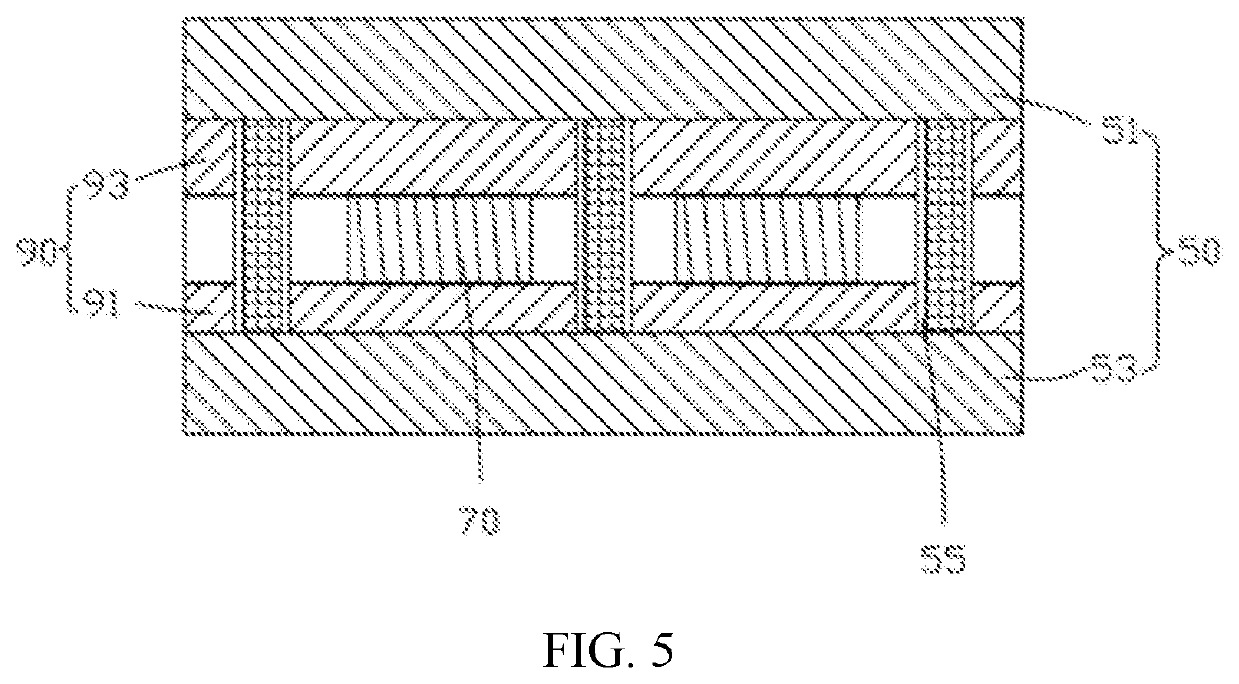
[0017]Please refer to the figures in the drawings, in which, like numbers refer to like elements throughout the description of the figures. Hereinafter, the present invention will be described in further detail with reference to examples. It is to be understood, however, that these examples are for illustrative purposes only and are not intended to limit the scope of the present invention.

[0018]Directional terms mentioned in the present invention, such as up, down, top, bottom, front, back, left, right, inside, outside, side, peripheral, center, horizontal, horizontal, vertical, longitudinal, axial, radial, the uppermost layer, or the lowermost layer, etc., are merely directions with reference to the drawings. Therefore, the directional terms used are for explaining and understanding the present invention, but not for limiting the present invention. In addition, for structural elements with the same or similar characteristics, the present invention uses the same reference numerals f...


PUM

PropertyMeasurementUnit
voltageaaaaaaaaaa
thicknessaaaaaaaaaa
brightnessaaaaaaaaaa

Abstract

The present invention provides an active matrix organic light emitting diode display panel including a display area with a recessed space and a concave area, wherein the concave area is connected to the display area and is disposed close to the recessed space, and the concave area is provided with an RC compensation capacitor therein, which is formed by voltage lines and a scanning lines. The active matrix organic light-emitting diode display panel provided by the present invention can reduce the phenomenon of screen-splitting between the concave area and the display area on the premise of ensuring a narrow upper frame.

Description

BACKGROUND OF INVENTIONField of Invention[0001]The present invention relates to a field of display technology, and in particular, to a notch active matrix organic light-emitting diode display panel capable of realizing a design of a narrow upper bezel.Description of Prior Art[0002]A design of a notch active matrix organic light-emitting diode display panel is a design scheme to increase a screen-to-body ratio of a mobile phone terminal. Generally, a concave cut design is used at an upper bezel of the active matrix organic light-emitting diode display panel for placement of a camera and other sensing devices. The design of the concave active matrix organic light-emitting diode display panel is characterized by a large difference in a number of pixels between different rows of the concave area, especially the difference between the two rows of pixels at the boundary between the concave area and the display area, which eventually results in a significant difference in brightness betwee...

Claims


Application Information

Patent Timeline
Patent Type & Authority Applications(United States)
IPC IPC(8): H01L27/32
CPCH01L27/3276H10K59/131
Inventor CHEN, TAO
Owner WUHAN CHINA STAR OPTOELECTRONICS SEMICON DISPLAY TECH CO LTD
Why Eureka
Try Eureka