Display panel and terminal device thereof

a terminal device and display panel technology, applied in semiconductor devices, diodes, electrical devices, etc., can solve the problems of inability to increase the screen of the mobile phone indefinitely, the range of the upper border cannot be continuously reduced, and the range of the lighting area of the camera can be limited, so as to achieve the effect of reducing the density of the pixel array in the device array layer in the area, greatly improving the light transmittance of the area, and improving the effect of display area

Inactive Publication Date: 2021-10-28
WUHAN CHINA STAR OPTOELECTRONICS SEMICON DISPLAY TECH CO LTD
View PDF0 Cites 2 Cited by
  • Summary
  • Abstract
  • Description
  • Claims
  • Application Information

AI Technical Summary

Benefits of technology

[0032]Compared with the prior art, the beneficial effects of the present invention are as follows. The invention relates to a display panel which is formed in a specific area of a substrate layer, for example, a camera area, by using a transparent PI material according to the present invention, so that the light transmittance of the area is greatly improved, and so that the camera disposed underneath can get enough light for normal shooting operations. At the same time, the density of the pixel array in the device array layer in the area is reduced, so that the area still has display function. In this way, the display panel according to the present invention has an effective display area as a whole, and there is no non-display area that is compromised to maintain the normal shooting function of the camera below. Thus, to a certain extent, a ‘full-screen’ display effect with high demand on the market is realized. The display effect of the ‘full screen’ obviously improves the satisfaction of the customer who uses the terminal device. Therefore, the display panel according to the present invention can be considered as a development trend of the panel industry.
[0033]Further, the pixel definition layer in the unit array layer of the camera area replaces the conventional organic photoresist with the novel functional material, black organic photoresist, according to the present invention. The black photoresist material has absorption properties for light, so that it can play a certain occlusion. Thereby, the phenomenon of the diffraction and reflection of the incident light, caused by the metal wiring in the device array layer, is effectively improved at the position of the camera. The light-leakage phenomenon between different pixels in the light-emitting area can be improved at the same time.
[0034]More importantly, due to the light-shielding effect of the black photoresist material introduced, if the pixel definition layer of the overall display area of the display panel adopts the photoresist material according to the present invention, the process of the display panel according to the present invention eliminates the need for a subsequent process of the polarizing plate of light. Thus, the manufacturing process of the display panel according to the present invention is simplified.
[0035]In addition, the display panel of the present invention does not need to use a laser cutting method to realize the normal shooting operation of the camera under the screen by the special shaped screen commonly used in the prior art, thereby avoiding the increase in the number of particles and the risk of a crack during the laser process for the screen. At the same time, the invention does not increase the cost of equipment, and is more conducive to future mass production.

Problems solved by technology

However, considering convenience of operation, the screen of the mobile phone cannot be increased indefinitely.
However, since a front camera of the mobile phone is generally placed in the upper-border area of the display screen, in order to ensure shooting requirements of the camera, the range of the upper border cannot be continuously reduced, and only the range of lighting area of the camera can be limited.
However, regardless of the design, the camera disposed under the display screen is in a non-display area of the display screen, so that there is always a non-display area within the effective display range of the display screen.

Method used


Image

  • Display panel and terminal device thereof
  • Display panel and terminal device thereof

Examples


Embodiment Construction

[0041]Technical solutions of a display panel and its terminal device according to the present invention will be further described in detail below with reference to the accompanying drawings and embodiments.

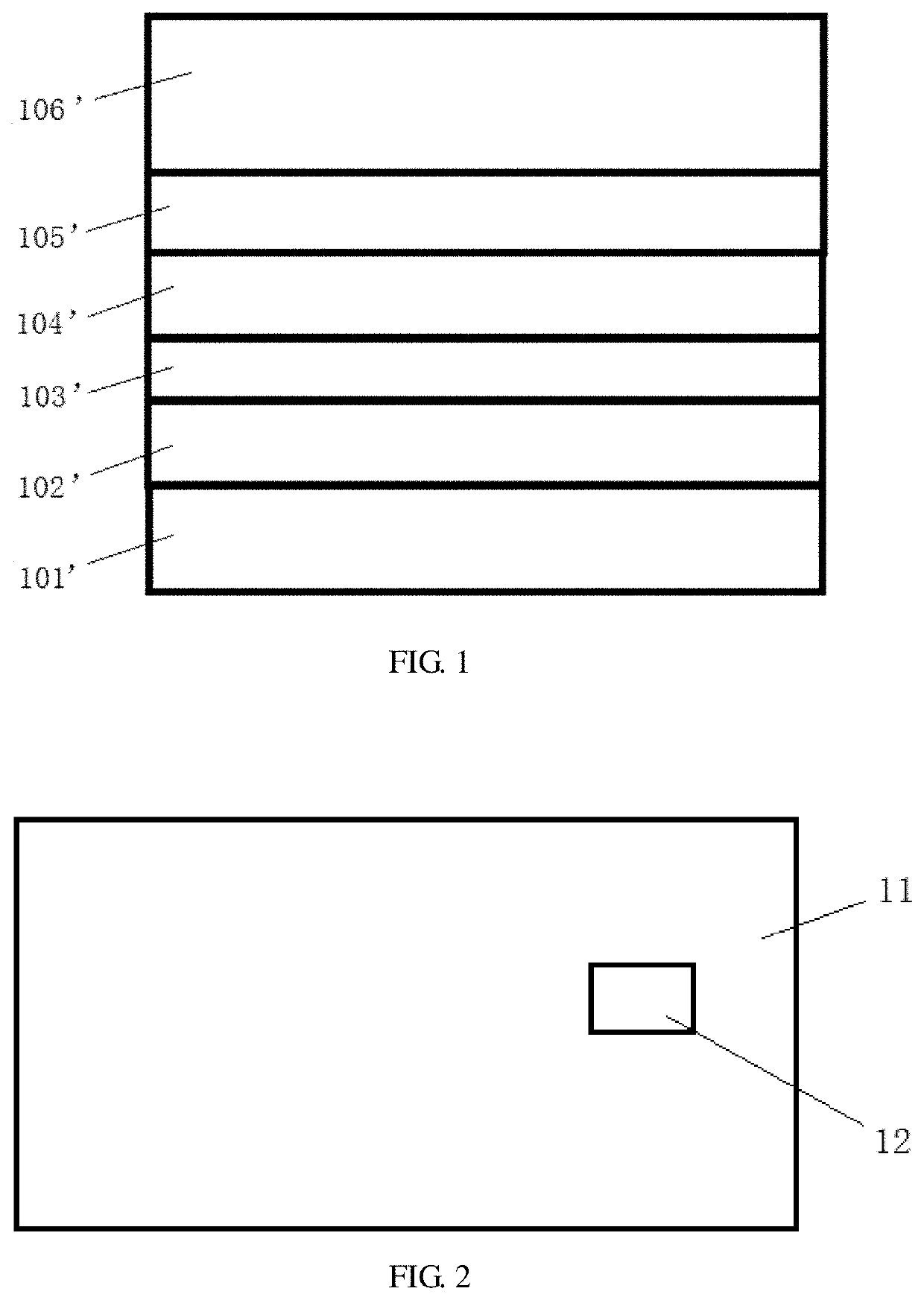
[0042]Referring to FIG. 2, an embodiment of the present invention provides a display panel defining a first display area 11 and a second display area 12. The first display area 11 may be, for example, an AA display area in a so-called display panel, and the second display area 12 may be a display panel area corresponding to a camera on the screen.

[0043]As shown in the figure, the first display area is completely wrapped around 4 surfaces of the second display area. In other embodiments, the first display area may be wrapped around 3 surfaces of the second display area, or both display areas may be arranged in parallel connection, which may be determined according to actual needs, and is not limited. In addition, in other embodiments, the number of the first display areas 11 and th...


PUM

PropertyMeasurementUnit
transmittanceaaaaaaaaaa
ODaaaaaaaaaa

Abstract

A display panel is provided. It defines a first display area and a second display area, including a substrate layer; the substrate layer includes a first portion, whose location is corresponding to the first display area, and a second portion, whose location is corresponding to the second display area. The second portion of the substrate layer can achieve a transmittance of 80% or more for an entire visible light band. A display panel provided is capable of performing an entire full-screen display, with high light transmittance without a significant non-display area.

Description

FIELD OF INVENTION[0001]The invention relates to the field of light-emitting display technology, in particular to a display panel and a terminal device thereof.BACKGROUND OF INVENTION[0002]It is known that with continuous advancement of technology, touch-screen mobile phones have become indispensable tools for people's daily lives. However, considering convenience of operation, the screen of the mobile phone cannot be increased indefinitely. On the contrary, it is sometimes limited to a certain size. Therefore, this requires a possible increase in a display range within a limited size range. That is, Industry often calls “narrow border” design in order to achieve a larger screen ratio of mobile phones.[0003]Among them, common practice in the industry is to reduce the border area of the display screen. The most effective way to reduce the lower border is pad bending technology, a fan-shaped area (Fanout), a wiring area, a driver IC, and a FPC in a part of the screen being bent togeth...

Claims


Application Information

Patent Timeline
Patent Type & Authority Applications(United States)
IPC IPC(8): H01L27/32H01L51/52
CPCH01L27/3234H01L51/5262H01L27/326H01L27/1218H10K59/121H10K59/122H01L27/12H04M1/02H10K59/65H10K59/00H10K50/85
Inventor BAI, SIHANG
Owner WUHAN CHINA STAR OPTOELECTRONICS SEMICON DISPLAY TECH CO LTD
Why Eureka
Try Eureka