
Array substrate, liquid crystal display device, electronic device

a liquid crystal display and substrate technology, applied in non-linear optics, instruments, optics, etc., can solve the problems of low contrast, slow response speed, liquid crystal display devices, etc., and achieve the effect of improving display quality and effective display area

Inactive Publication Date: 2013-04-02
SHARP KK
View PDF46 Cites 1 Cited by
  • Summary
  • Abstract
  • Description
  • Claims
  • Application Information

AI Technical Summary

Benefits of technology

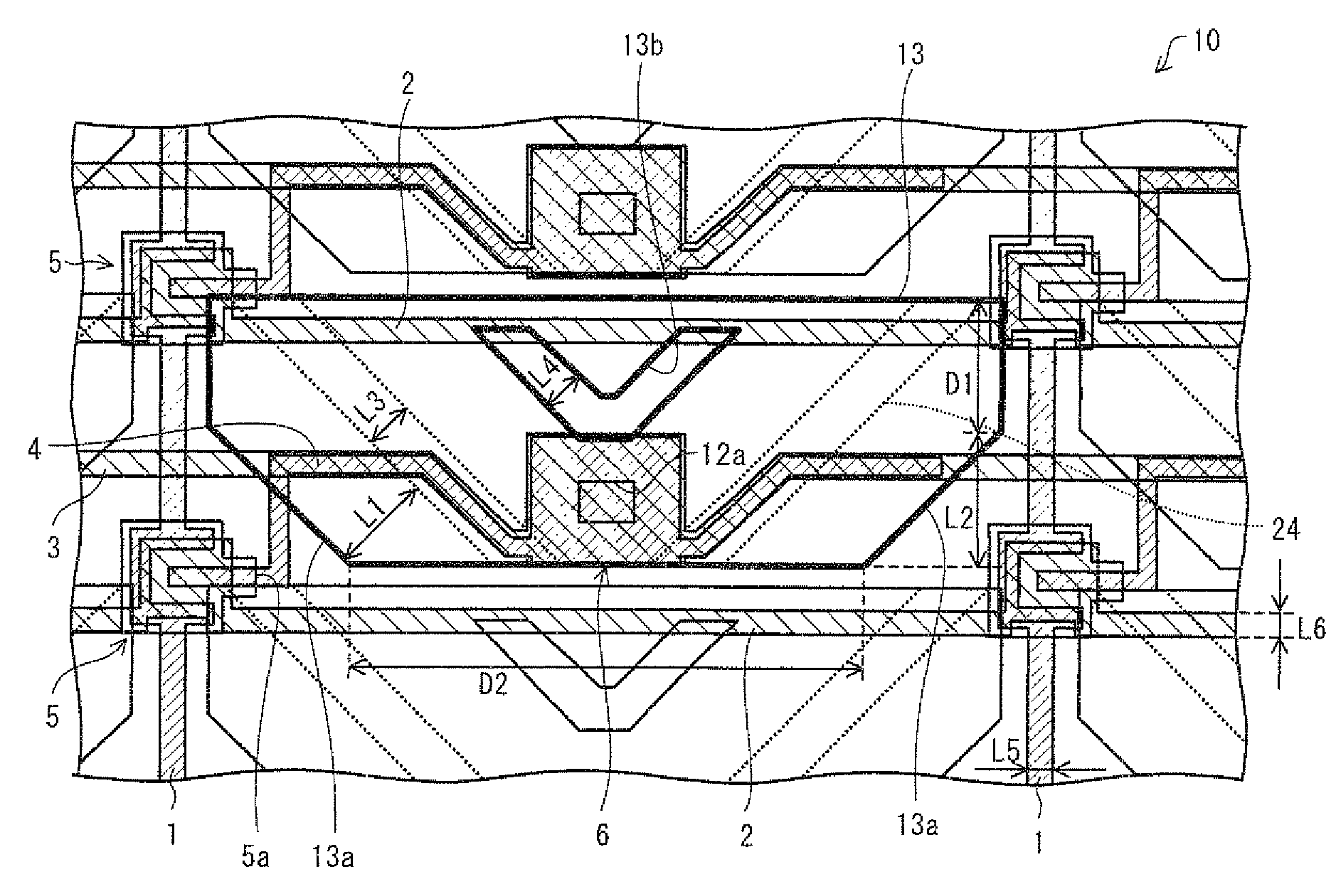
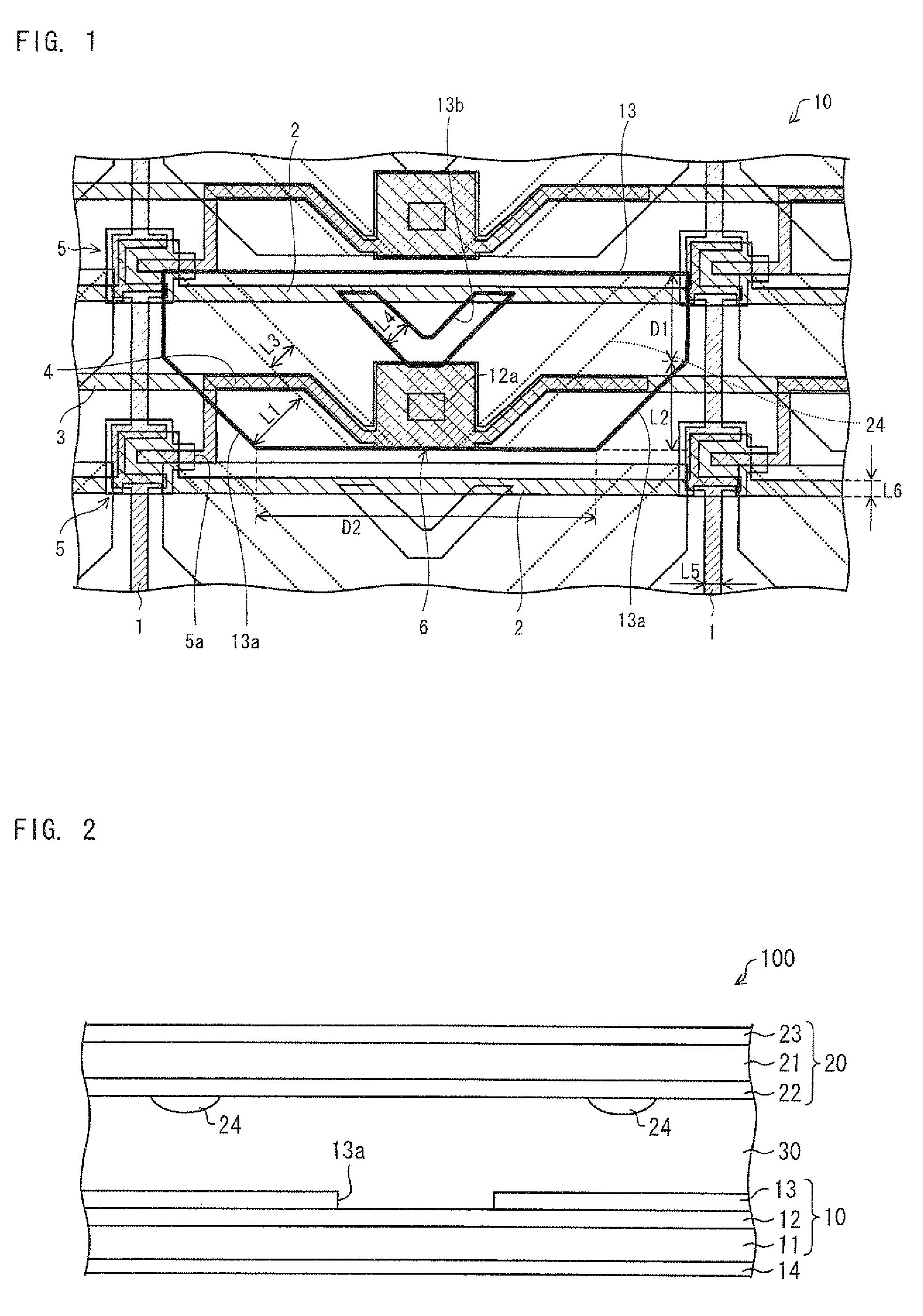
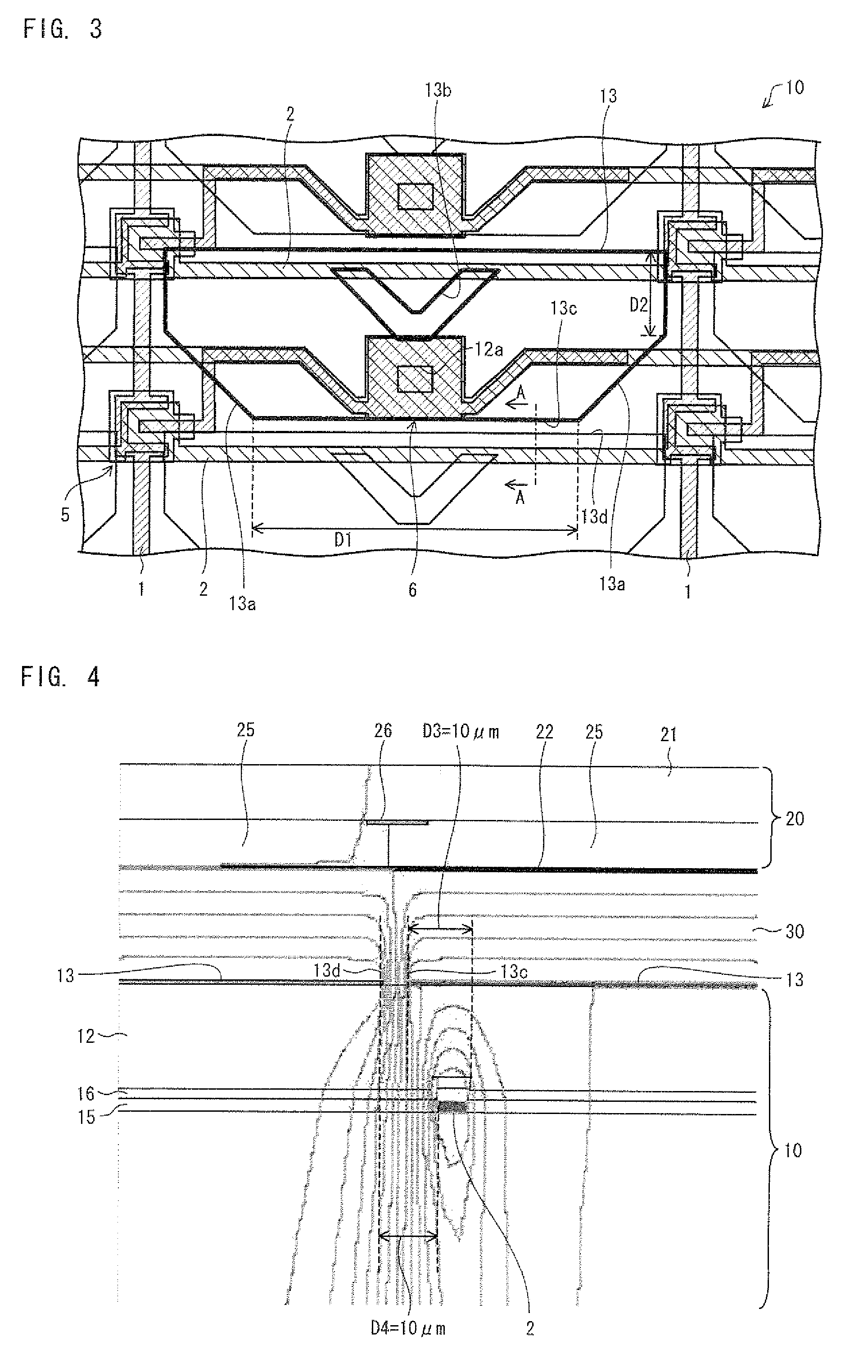
This patent describes an array substrate for a liquid crystal display that improves display quality by dividing one picture element region into multiple sections and aligning liquid crystal molecules in different directions in each section. The array substrate includes a plurality of scanning lines and data lines, and a plurality of substantially rectangular picture element electrodes that are connected to the scanning and data lines. Each picture element electrode has two corners that serve as alignment dividing means, ensuring an effective display area in one picture element. The technical effect of this invention is to optimize the display quality of liquid crystal displays.

Problems solved by technology

Liquid crystal display devices have problems such as a low contrast, a slow response speed, a narrow viewing angle and the like.
This causes a problem such that, if the effective display area is ensured, it becomes difficult to provide a large storage capacitance.
In a case where the parasitic capacitance (Csd) between the picture element electrode and the data line becomes lager as described above, there arises a problem of deterioration in display quality, such as shadowing, uneven display within a panel plane, and the like.

Method used


Image

  • Array substrate, liquid crystal display device, electronic device
  • Array substrate, liquid crystal display device, electronic device
  • Array substrate, liquid crystal display device, electronic device

Examples


Embodiment Construction

[0051]The following explains one embodiment of the present invention. Note that the present embodiment explains a liquid crystal display device (hereinafter, referred to as an MVA liquid crystal display device) of an MVA (Multidomain Vertical Alignment) mode in which one picture element region is divided into a plurality of domains. Further, note that one picture element region does not indicate only a region corresponding to a picture element electrode directly connected to a switching element, but does include a region of a sub-picture element electrode connected via a coupling capacitance to a switching element or a picture element connected to the switching element. The one picture element region also includes a region in a case where the picture element electrode and the sub-picture element electrode each connected to the switching element are viewed as one unit.

[0052]As shown in FIG. 2, the MVA liquid crystal display device of the present embodiment includes an array substrate...


PUM

PropertyMeasurementUnit
cut distanceaaaaaaaaaa
sizeaaaaaaaaaa
sizeaaaaaaaaaa

Abstract

An array substrate of the present invention includes: an insulating substrate; a plurality of scanning lines on the insulating substrate; a plurality of data lines each disposed so as to intersect the plurality of scanning lines on the insulating substrate; picture element electrodes each formed in a substantially rectangular shape, the picture element electrodes each being connected, via a switching element, to a corresponding scanning line and a corresponding data line, the picture element electrodes each having a long side disposed along a direction in which the plurality of scanning lines are extended and a short side disposed along a direction in which the plurality of data lines are extended, the picture element electrodes each having cut sections formed by cutting two corners of each of the picture element electrodes, the cut sections being formed so as to serve as alignment dividing means. This makes it possible, regarding an MVA liquid crystal display device, to easily ensure a sufficient process yield as well as improving display quality by ensuring a sufficient aperture ratio in each one pixel.

Description

[0001]This application is the U.S. national phase of International Application No. PCT / JP2009 / 067572, filed 8 Oct. 2009, which designated the U.S. and claims priority to Japan Application No. 2009-031789, filed 13 Feb. 2009, the entire contents of each of which are hereby incorporated by reference.TECHNICAL FIELD[0002]The present invention relates to an array substrate provided in an MVA (Multi-domain Vertical Alignment) liquid crystal display device.BACKGROUND ART[0003]Liquid crystal display devices have problems such as a low contrast, a slow response speed, a narrow viewing angle and the like. For solving these problems, various techniques have been proposed.[0004]For example, in a method called a Vertical Alignment (VA) mode, liquid crystal molecules of liquid crystals having a negative dielectric anisotropy are aligned in a vertical direction by use of a vertical alignment film in a case where voltage is not applied to the liquid crystals. As a result, a black display is carrie...

Claims


Application Information

Patent Timeline
Patent Type & Authority Patents(United States)
IPC IPC(8): G02F1/1337
CPCG02F1/134309G02F1/1393G02F1/133707G02F2201/40G02F2001/13606G02F1/136213G02F1/13606
Inventor YOSHIDAHORIUCHI, SATOSHIYAMADA, TAKAHARUHISADA, YUHKOITOH, RYOHKI
Owner SHARP KK
Learn More