This helps you quickly interpret patents by identifying the three key elements:
Problems solved by technology
Method used
Benefits of technology
Benefits of technology
The present disclosure provides a fingerprint sensing module with better resistance to external forces. By adding microlenses and a spacer pattern between the substrates, the tolerance of external force and process margin are increased, leading to higher production yield and reliability. The flat layer carrying the spacer pattern also improves the utilization of light energy for sensing, resulting in better overall sensing sensitivity.
Problems solved by technology
However, such fingerprint sensing module is prone to receive stray light incident at a large angle due to the large spacing between the microlenses, which makes the fingerprint images blurry.
In addition, when the user presses the display panel to perform fingerprint recognition, the curved display panel also increases the risk of crushing the microlenses, reducing the reliability of long-term operation.
Method used
Image
Click on the blue label to locate the original text in one second.
Reading with bidirectional positioning of images and text.
Examples
first embodiment
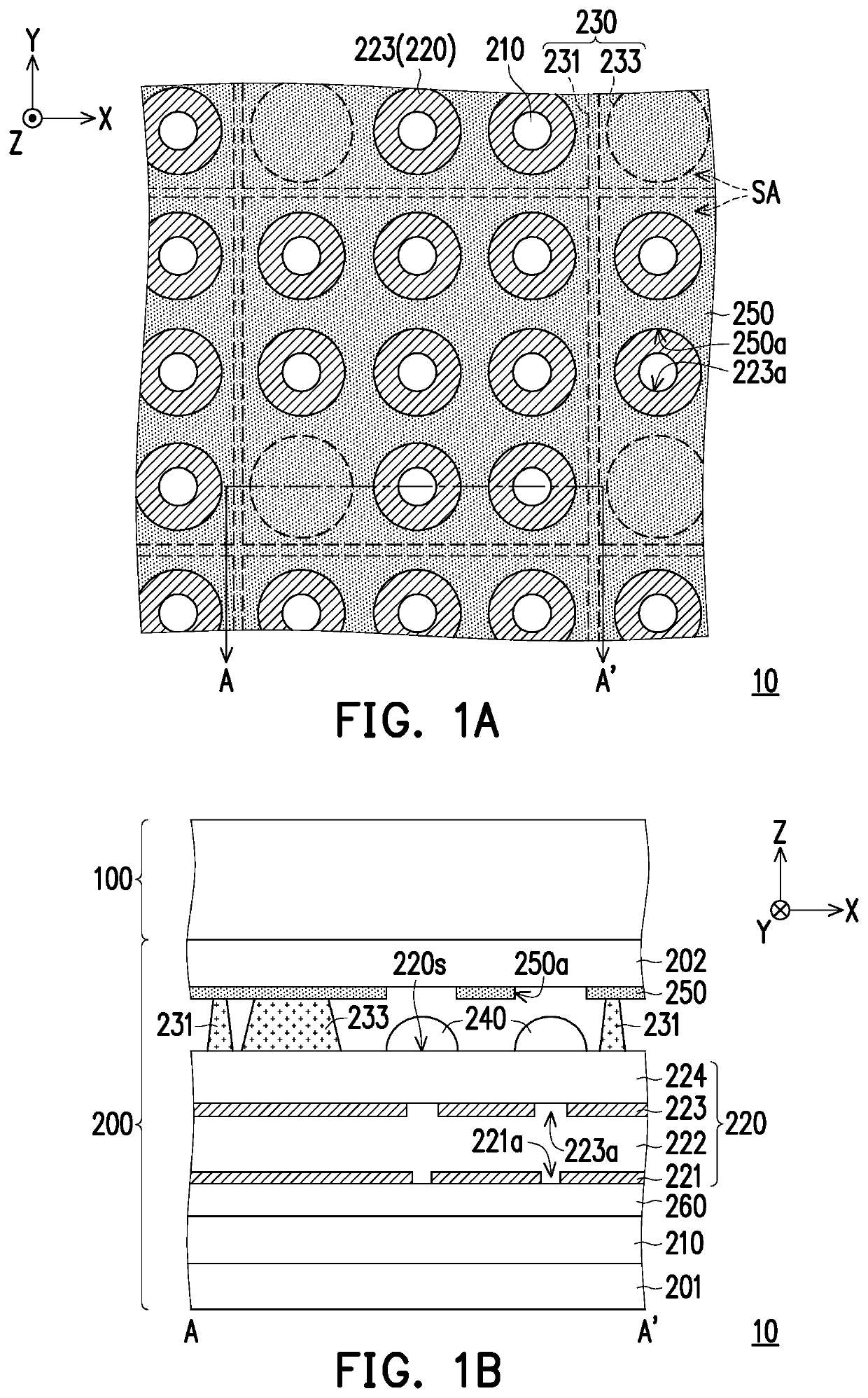
[0056]FIG. 1A is a schematic top view of a display apparatus according to the disclosure. FIG. 1B is a schematic cross-sectional view of the display apparatus of FIG. 1A. FIG. 1B corresponds to a section line A-A′ of FIG. 1A. For the sake of clarity, FIG. 1A only shows a photosensitive element layer 210, a light-shielding pattern layer 223 of a collimation structure layer 220, a spacer pattern 230, and a light-shielding pattern layer 250 of FIG. 1B.
[0057]In FIG. 1A and FIG. 1B, a display apparatus 10 includes a display panel 100 and a fingerprint sensing module 200. The fingerprint sensing module 200 is adapted to overlap the display panel 100 and has a plurality of sensing pixel areas SA. The sensing pixel areas SA may be disposed in an array. For example, the sensing pixel areas SA may be disposed in multiple columns and multiple rows that are respectively in a direction X and a direction Y. In this embodiment, the fingerprint sensing module 200 may be disposed on the back side of...
second embodiment
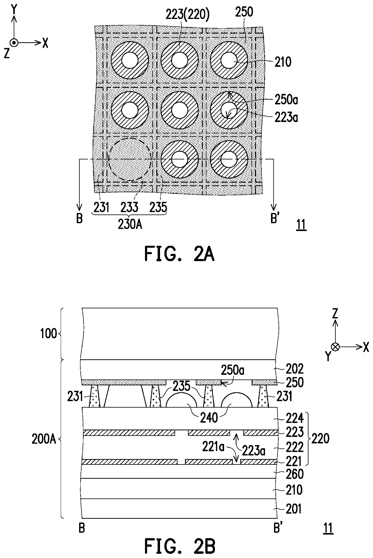
[0069]FIG. 2A is a schematic top view of a display apparatus according to the disclosure. FIG. 2B is a schematic cross-sectional view of the display apparatus of FIG. 2A. FIG. 2B corresponds to a section line B-B′ of FIG. 2A. For the sake of clarity, FIG. 2A only shows a photosensitive element layer 210, a light-shielding pattern layer 223 of a collimation structure layer 220, a spacer pattern 230A, and a light-shielding pattern layer 250 of FIG. 2B.
[0070]In FIG. 2A and FIG. 2B, the difference between the display apparatus 11 of this embodiment and the display apparatus 10 of FIG. 1A lies in the arrangement of the spacer pattern. Specifically speaking, the spacer pattern 230A of the display apparatus 11 further extends between any adjacent two of a plurality of microlenses 240 in each of the sensing pixel areas SA. For example, in this embodiment, the spacer pattern 230A further includes a plurality of extension portions 235 extending between the microlenses 240 and a plurality of c...
fifth embodiment
[0077]FIG. 5A is a schematic top view of a display apparatus according to the present disclosure. FIG. 5B is a schematic cross-sectional view of the display apparatus of FIG. 5A. FIG. 5B corresponds to a section line D-D′ of FIG. 5A. For the sake of clarity, FIG. 5A only shows a photosensitive element layer 210, a light-shielding pattern layer 223 of a collimation structure layer 220A, a spacer pattern 230C, and a plurality of microlenses 240A of FIG. 5B.
[0078]In FIG. 5A and FIG. 5B, the main difference between a display apparatus 20 of this embodiment and the display apparatus 10 of FIG. 1A lies in the arrangement of the spacer pattern. Specifically, the spacer pattern 230C of a fingerprint sensing module 200D of the display apparatus 20 may selectively overlap part of the microlens 240A in a direction Z.
[0079]For example, in this embodiment, the microlenses 240A may be divided into a plurality of first microlenses 241 and a plurality of second microlenses 242, and the first microl...
PUM
Abstract
A fingerprint sensing module includes a first substrate, an active device, a photosensitive element layer, a collimation structure layer, a second substrate, a plurality of micro lenses, and a spacer pattern. The active device is disposed on the first substrate. The photosensitive element layer is disposed on the first substrate and is electrically connected to the active device. The collimation structure layer is disposed on the photosensitive element layer. The second substrate is disposed on the collimation structure layer. The micro lenses are disposed on a surface of the collimation structure layer facing away from the photosensitive element layer, and overlap the photosensitive element layer. The micro lenses are divided into a plurality of microlens groups, and the microlens groups are respectively located in a plurality of sensing pixel areas of the fingerprint sensing module. The spacer pattern extends between the microlens groups.
Description
CROSS-REFERENCE TO RELATED APPLICATION[0001]This application claims the priority benefits of U.S. provisional application Ser. No. 63 / 066,391, filed on Aug. 17, 2020, U.S. provisional application Ser. No. 63 / 070,880, filed on Aug. 27, 2020, Taiwan application serial no. 110104319, filed on Feb. 4, 2021, and Taiwan application serial no. 110113292, filed on Apr. 13, 2021. The entirety of each of the above-mentioned patent applications is hereby incorporated by reference herein and made a part of this specification.BACKGROUNDTechnical Field[0002]The disclosure relates to a sensing module, and particularly to a fingerprint sensing module.Description of Related Art[0003]To increase the screen-to-body ratio of the display to achieve a narrow bezel design, under-display fingerprint sensing technology has become a trend. To put it simply, the under-display fingerprint sensing technology is to dispose a fingerprint sensing module under a display panel of an electronic apparatus. After the e...
Claims
Application Information
Patent Timeline
Application Date:The date an application was filed.
Publication Date:The date a patent or application was officially published.
First Publication Date:The earliest publication date of a patent with the same application number.
Issue Date:Publication date of the patent grant document.
PCT Entry Date:The Entry date of PCT National Phase.
Estimated Expiry Date:The statutory expiry date of a patent right according to the Patent Law, and it is the longest term of protection that the patent right can achieve without the termination of the patent right due to other reasons(Term extension factor has been taken into account ).
Invalid Date:Actual expiry date is based on effective date or publication date of legal transaction data of invalid patent.

