Capacitor in semiconductor device and method of manufacturing the same

Inactive Publication Date: 2007-01-04
SK HYNIX INC
View PDF6 Cites 9 Cited by
  • Summary
  • Abstract
  • Description
  • Claims
  • Application Information

AI Technical Summary

Benefits of technology

[0015] Therefore, the present invention has been made in view of the above problems, and it is an object of the present invention to provide a capacitor in semiconductor device and method of manufacturing of the same, capable of easily securing capacitance of the capacitor, decreasing leakage current, and increasing breakdown voltage, thereby improving process yield and reliability of device operation, via use of an alumina (Al2O3) film having a high dielectric constant as a dielectric film of a capacitor and use of an aluminum (Al) layer as an electrode.

Problems solved by technology

Recently, the high degree of integration of semiconductor devices has led to a decrease in cell size, and, as a result, it has become more difficult to fabricate a capacitor having sufficient capacitance.
However, such methods suffer from problems and disadvantages.
That is, a great deal of research has been focused on dielectric substances having a high dielectric constant, for example, tantalum oxide (Ta2O5), titanium oxide (TiO2) and strontium titanate (SrTiO3), but it is difficult to apply these materials to practical devices due to the absence of solid confirmation of reliability such as breakdown voltage and thin film characteristics.
In addition, decreasing the thickness of the dielectric film results in destruction thereof during operation of the device, this, in turn, significantly affects reliability of the capacitor.
Additionally, a method of increasing a surface area of a lower electrode of the capacitor by forming a poly-silicon layer into multi-layers and then forming the resulting multi-layers into a fin structure connecting each layer therethrough, or a method of increasing a height of the capacitor such as formation of a cylinder-shaped lower electrode on an upper part of a contact suffers from difficulty of subsequent processes due to a step caused by increased height of the capacitor, and high integration of DRAMs leads to a decreased area of the device, thus making it difficult to secure sufficient capacitance of the capacitor.
However, if the effective thickness of the nitride film is reduced to less than 40 Å, oxidation resistance thereof is sharply decreased, which results in problems such as oxidization of lower structures including lower electrode 12 and bit lines during a subsequent thermal oxidation process, increased leakage current of the capacitor itself and attenuation of breakdown voltage.
Further, as the upper / lower electrodes are formed of poly-silicon layers, there are additional problems such as degeneration of electrodes, and formation of oxide films on the dielectric film and electrode interfaces thus increasing the effective thickness of the oxide film and then decreasing capacitance.

Method used


Image

  • Capacitor in semiconductor device and method of manufacturing the same
  • Capacitor in semiconductor device and method of manufacturing the same
  • Capacitor in semiconductor device and method of manufacturing the same

Examples


Embodiment Construction

[0041] Hereinafter, a capacitor in semiconductor device and a method of manufacturing the same in accordance with the present invention will be described in more detail with reference to the accompanying drawings.

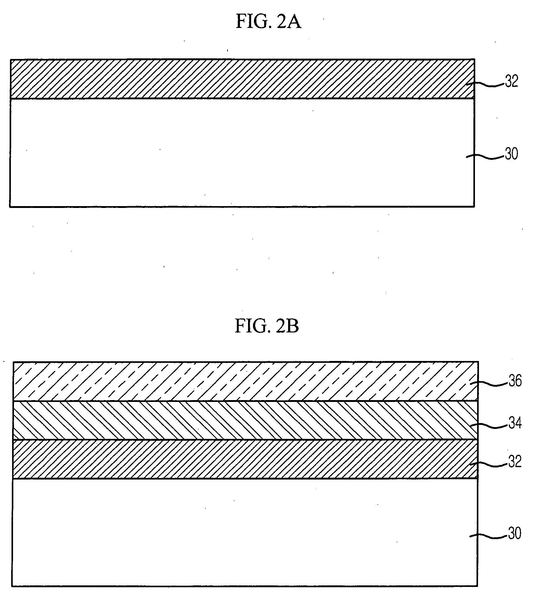
[0042]FIGS. 2a through 2c show a process flow chart for a capacitor in semiconductor device and a method of manufacturing the same in accordance with the present invention.

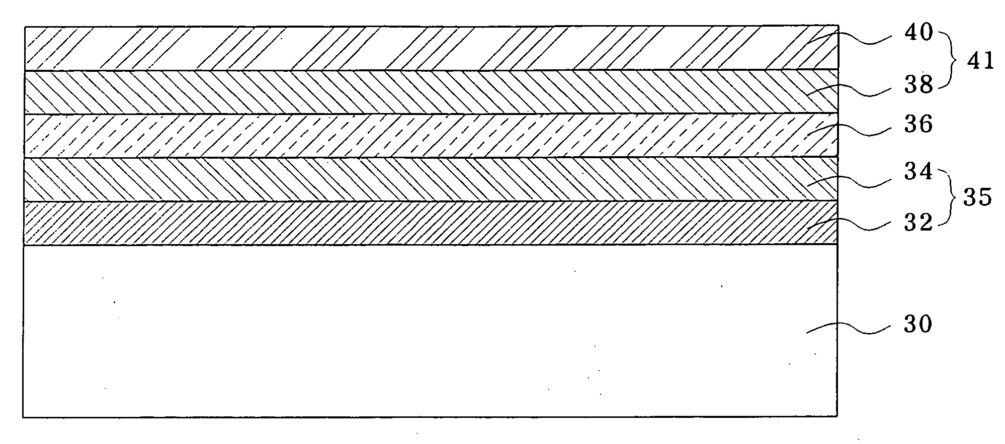
[0043] First, referring to FIG. 2a, lower structures such as element-isolation oxide films defining an active layer, MOSFET and bit lines are formed on a semiconductor substrate, although they are not shown in FIG. 2a. Next, a contact plug for the lower electrode is formed on the entire surface of the resulting structure. A first poly-silicon layer 32 for the lower electrode is formed on a semiconductor substrate 10 including the lower structures and the contact plug for the lower electrode. Herein, the first poly-silicon layer 32 may be deposited in the form into a doped silicon layer, an undoped silic...


PUM


Abstract

The present invention relates to a capacitor in semiconductor device and a method of manufacturing the same, wherein, owing to formation of a lower electrode and an upper electrode into a stack structure of a poly-silicon layer and an aluminum (Al) layer and formation of an alumina (Al2O3) film as a dielectric film, the lower electrode is formed into a stack structure of the poly-silicon layer-aluminum (Al) layer, thus increasing a surface area of electrodes due to the absence of oxidation during annealing, and preventing degeneration of the device, and use of the dielectric film including a high-dielectric constant material layer enables reduction of the dielectric film's thickness. Accordingly, the present invention is capable of increasing capacitance, is capable of reducing leakage current and improving dielectric breakdown characteristics via internal formation of an MIM capacitor, and is capable of reducing production costs by performing a continuous process via use of a single piece of equipment.

Description

BACKGROUND OF THE INVENTION [0001] 1. Field of the Invention [0002] The present invention relates to a capacitor in semiconductor device and a method of manufacturing the. More specifically, the present invention relates to a capacitor in semiconductor device and method of manufacturing of the same, wherein an alumina (Al2O3) film capable of further decreasing the effective thickness is used as a dielectric film, instead of a conventional nitride film, and an aluminum (Al) layer is used as a conductive film, thus enhancing the breakdown voltage of the capacitor and decreasing leakage current leading to improved reliability of the device. [0003] 2. Description of the Related Art [0004] Recently, the high degree of integration of semiconductor devices has led to a decrease in cell size, and, as a result, it has become more difficult to fabricate a capacitor having sufficient capacitance. Particularly, in dynamic random access memory (DRAM) devices consisting of a MOS transistor and a ...

Claims


Application Information

Patent Timeline
IPC IPC(8): H01L21/8242H01L29/94H01L21/20
CPCH01L28/40H01L21/31H01L27/04
Inventor LEE, EUN A.KIM, HAI WON
Owner SK HYNIX INC
Why Eureka
Try Eureka